How PCB Design Decisions Can Affect Manufacturing
PCB design decisions, from via placement to material selection, can significantly affect manufacturing time, complexity and efficiency, making early DFM input essential.

High-technology PCB manufacturing for 5G infrastructure, wireless connectivity, RF front-end systems, and network electronics. UK-based engineering and manufacturing from prototype through to production.
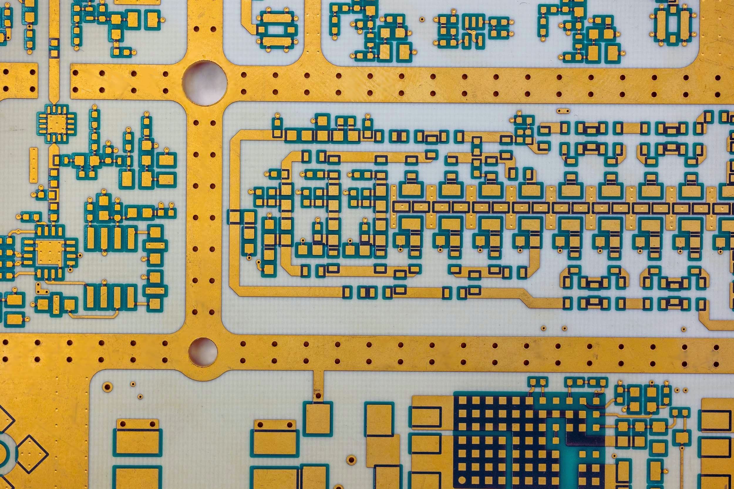
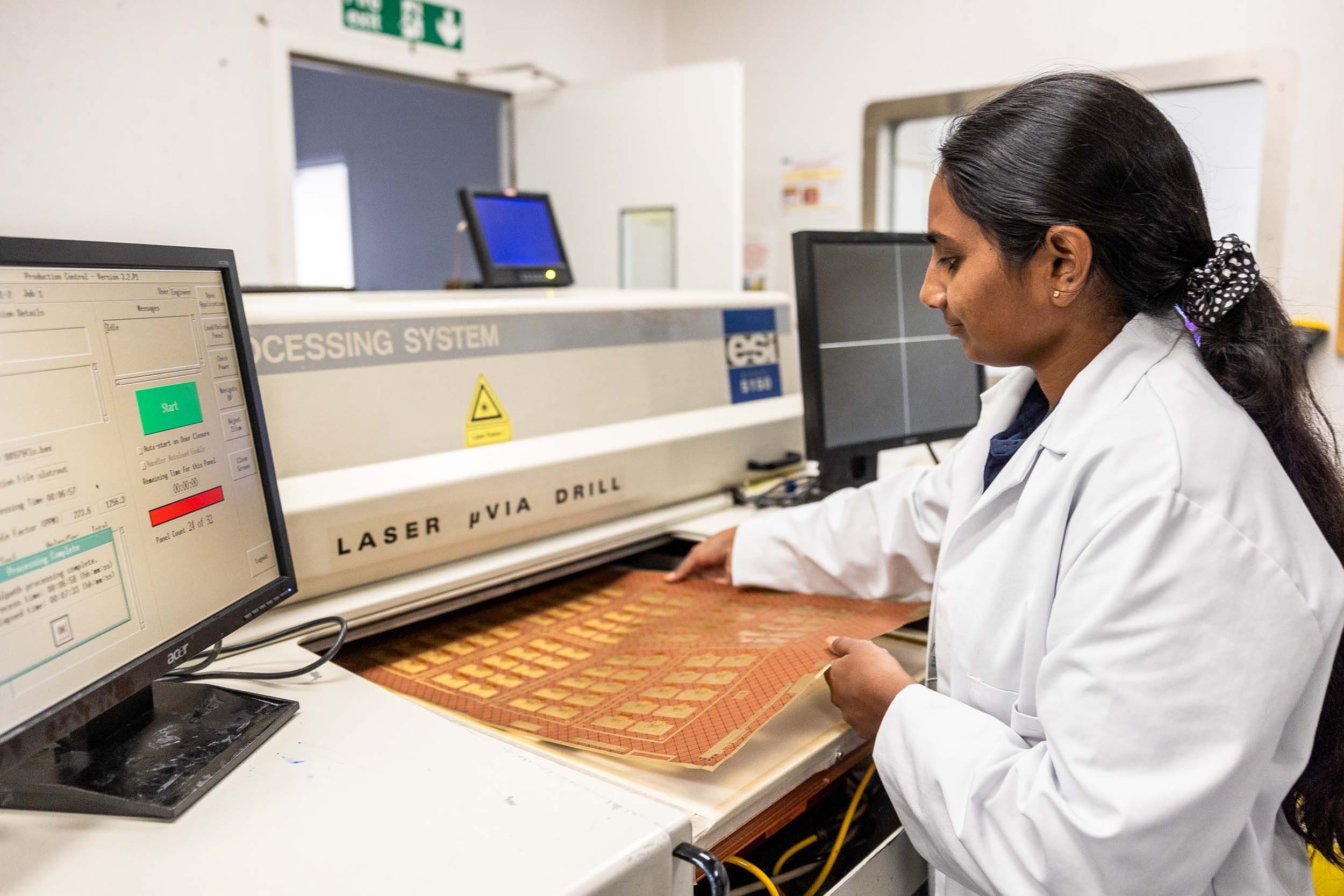
As a UK manufacturer of high-technology printed circuit boards for communications and network electronics, Exception PCB works with engineering teams developing 5G infrastructure, wireless platforms, IoT devices, and RF front-end systems.
Communications electronics demand precise control over signal behaviour. Small variations in impedance, material loss, or layer registration can affect system performance, network reliability, or compliance with frequency regulations. We build PCBs that deliver consistent controlled impedance, low-loss performance, and stable electrical behaviour across frequency and temperature, supporting programmes where RF performance is critical.

Whether you are developing 5G infrastructure, designing an RF front-end module, or scaling a wireless connectivity platform to production, our team is ready to support you.
Exception PCB supports a broad range of communications and network programmes, working with engineering and procurement teams from prototype through to production.
5G base stations and wireless network infrastructure demand PCBs that maintain stable RF performance across high-frequency bands with minimal signal loss. We build multilayer boards with controlled impedance routing, low-loss laminates, and tight layer registration to support the signal integrity and thermal management requirements of modern network electronics.
Phased array antennas, RF front-end modules, and microwave assemblies require precise impedance control, low insertion loss, and stable dielectric behaviour across operating frequencies. We manufacture multilayer and HDI boards using specialist low-loss materials including Rogers and PTFE-based laminates, with engineering input on stack-up design and routing strategies to optimise RF performance.
Wireless connectivity modules, smart meters, IoT gateways, and industrial network devices combine processing complexity with miniaturisation requirements. We support these applications with HDI builds, controlled impedance routing for wireless interfaces, and material selection that balances electrical performance with the volume and cost considerations of connected device programmes.
Routers, switches, network transport platforms, and test equipment require high-speed digital PCBs with consistent signal integrity across complex multilayer structures. We manufacture multilayer and HDI boards with controlled impedance routing for high-speed data paths, alongside stack-up guidance to support design teams working at the edge of signal performance.
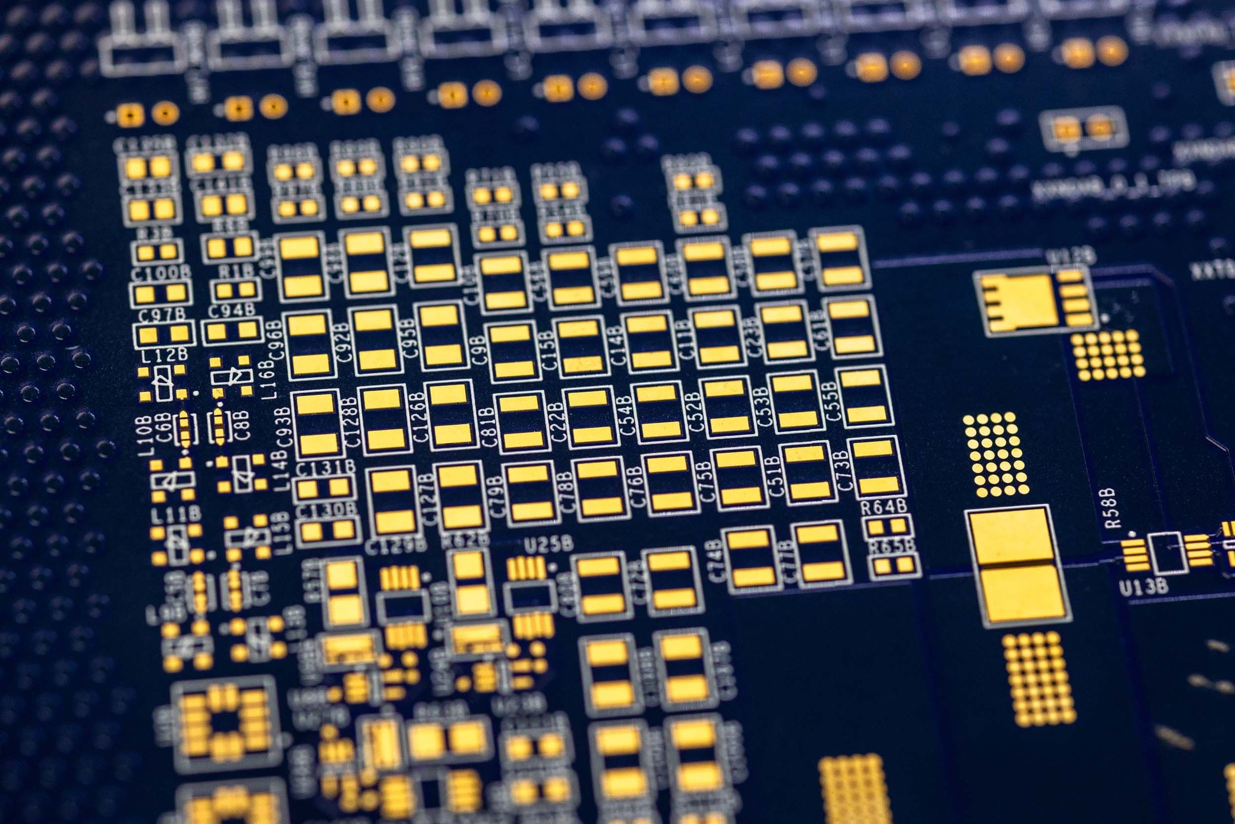
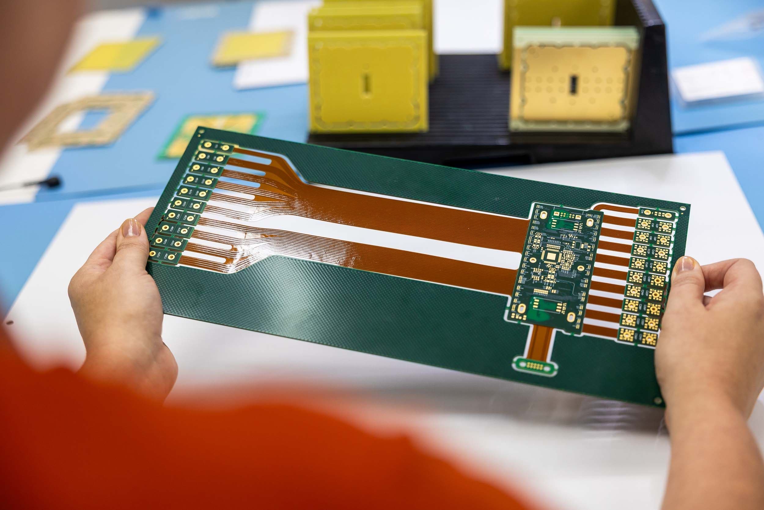
Communications electronics often push the limits of PCB materials and process capability. We offer a broad range of advanced technologies to support RF, high-speed digital, and mixed-signal designs.

Communications electronics operate in demanding environments and often require documented evidence of process control and build consistency. We apply rigorous quality management built on ISO 9001 and structured process control to support the traceability requirements of engineering and procurement teams.
WE PROVIDE:
This gives teams a clear, documented picture of build quality at every stage, from incoming materials through to final inspection.

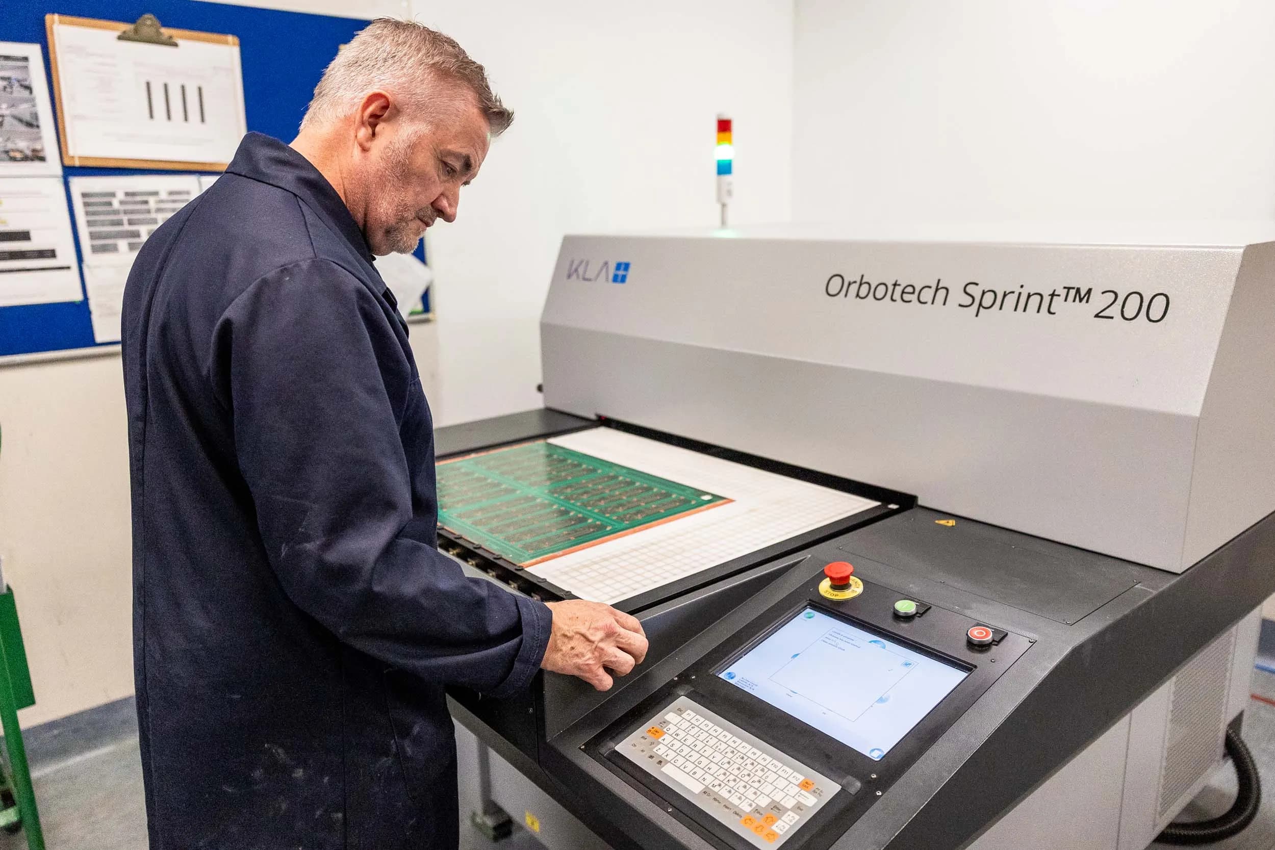
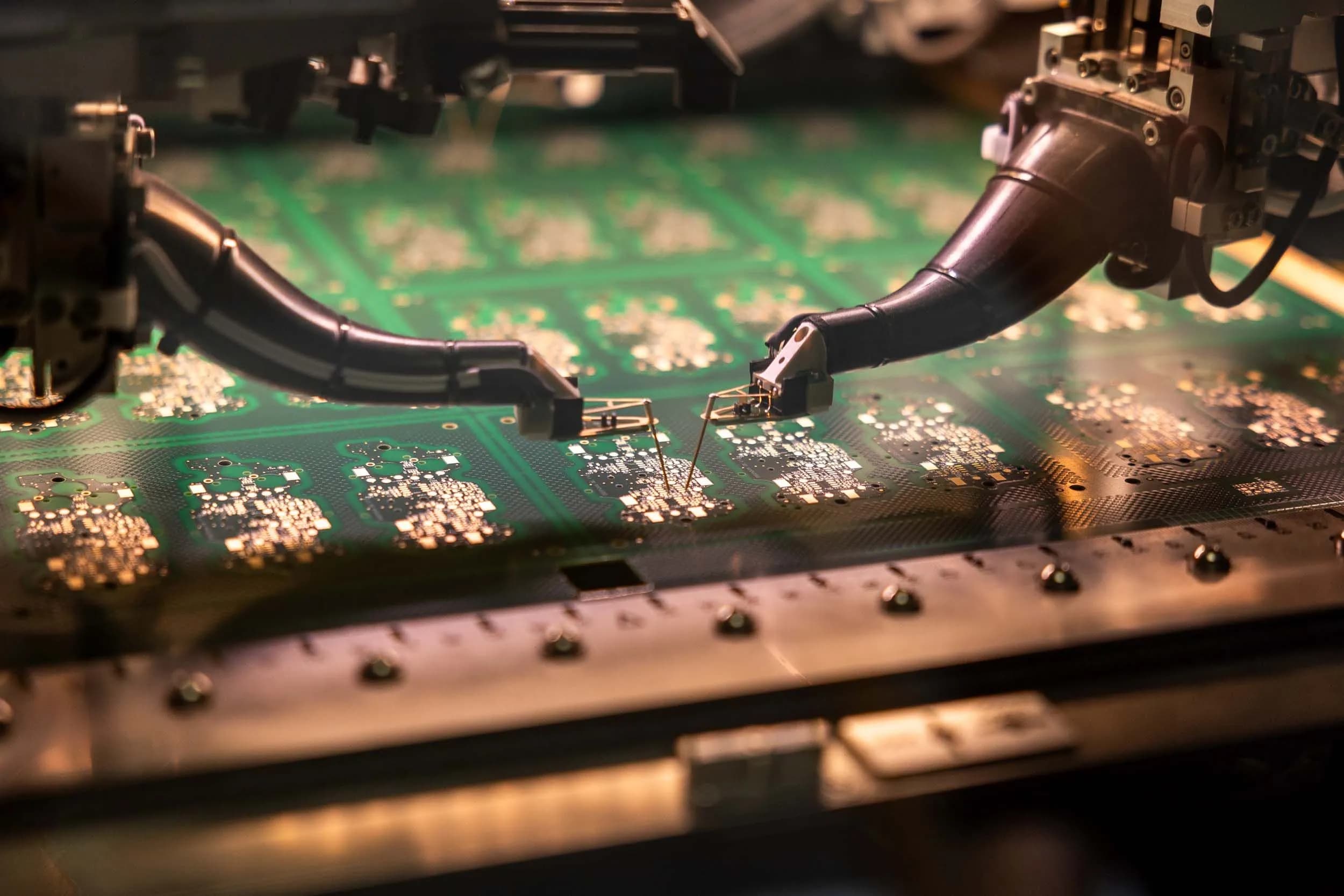
Every communications PCB we build passes through a structured inspection and test regime before it leaves our facility.
WE PROVIDE:
SPEAK TO OUR COMMUNICATIONS ENGINEERING TEAM
Whether you are developing next-generation network infrastructure, advancing an RF platform, or scaling a connected device to production, our team is ready to support your programme.