
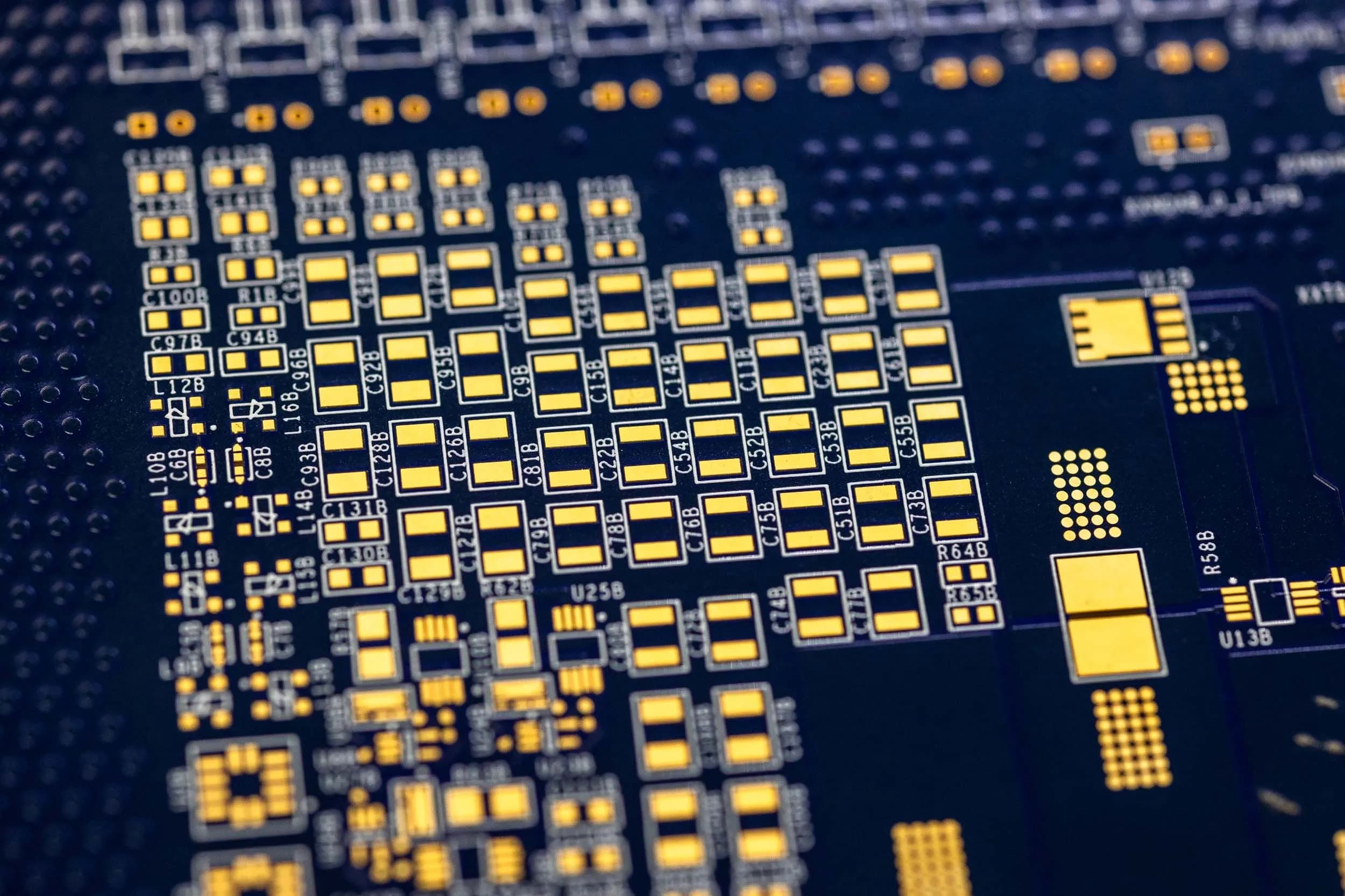
PCB TECHNOLOGY
Advanced PCB technologies for HDI, RF, flex, rigid-flex, via filling and specialist material requirements in complex PCB designs.
Exception PCB manufactures high-technology PCBs using advanced processes that support electrical performance, thermal stability, mechanical reliability and manufacturability.
Our capabilities include HDI, RF PCBs, flex and rigid-flex circuits, copper and resin via filling, and advanced PCB materials. Each technology is managed within a controlled UK manufacturing environment, helping engineering teams move from concept to production with greater confidence.
Search our technology pages to explore HDI, RF PCBs, flex and rigid-flex, via filling, advanced materials and supporting technical resources.
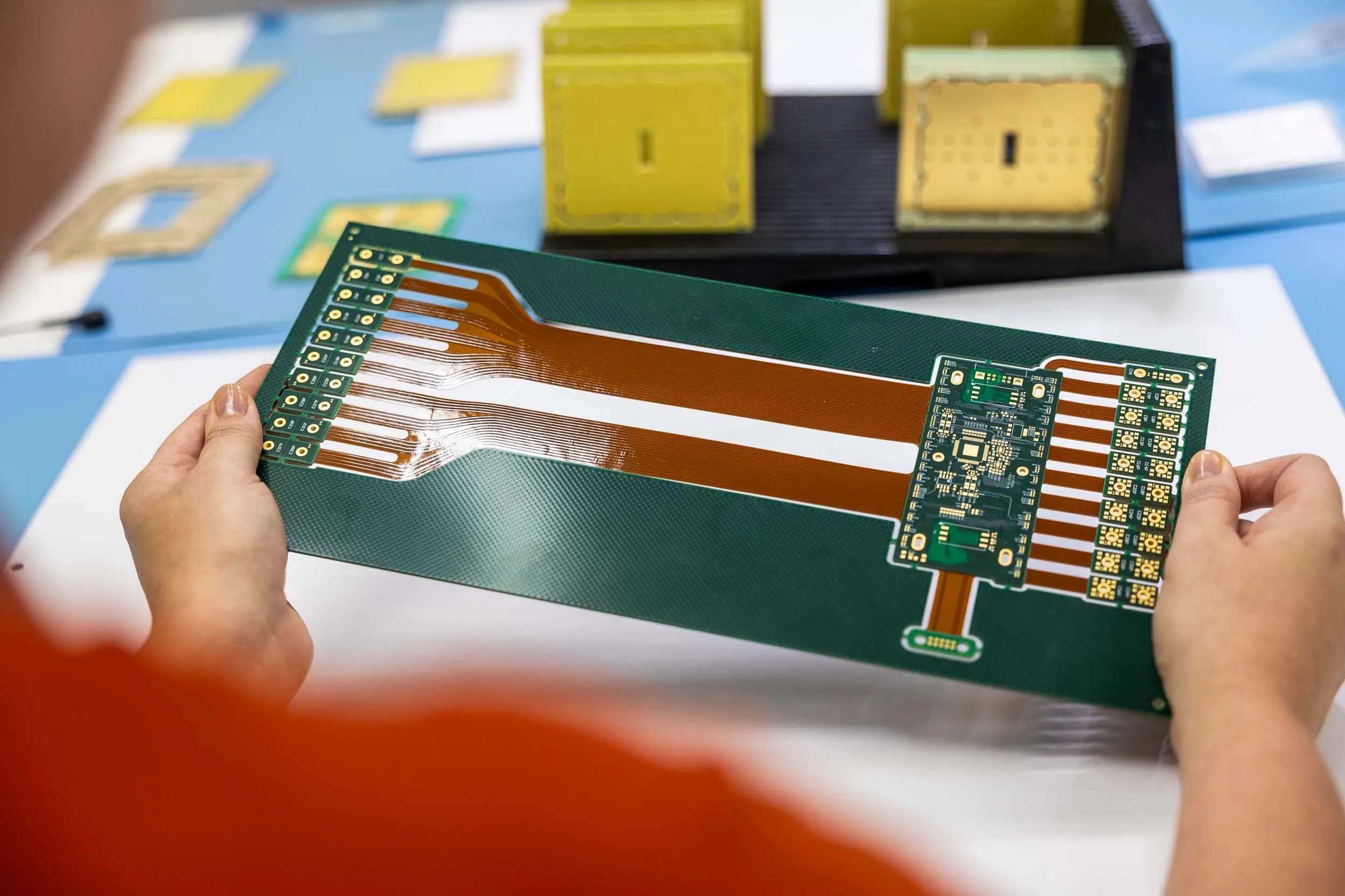
FLEX & FLEX-RIGID PCB CAPABILITY
Flex and rigid-flex PCB construction enables compact packaging, dynamic movement, and reduced interconnect complexity within advanced electronic assemblies.
Exception PCB manufactures flex and rigid-flex designs using controlled lamination, polyimide material systems, and precision registration to support demanding applications where reliability and space optimisation are critical.
These constructions are commonly used where traditional rigid boards introduce assembly constraints or mechanical limitations.
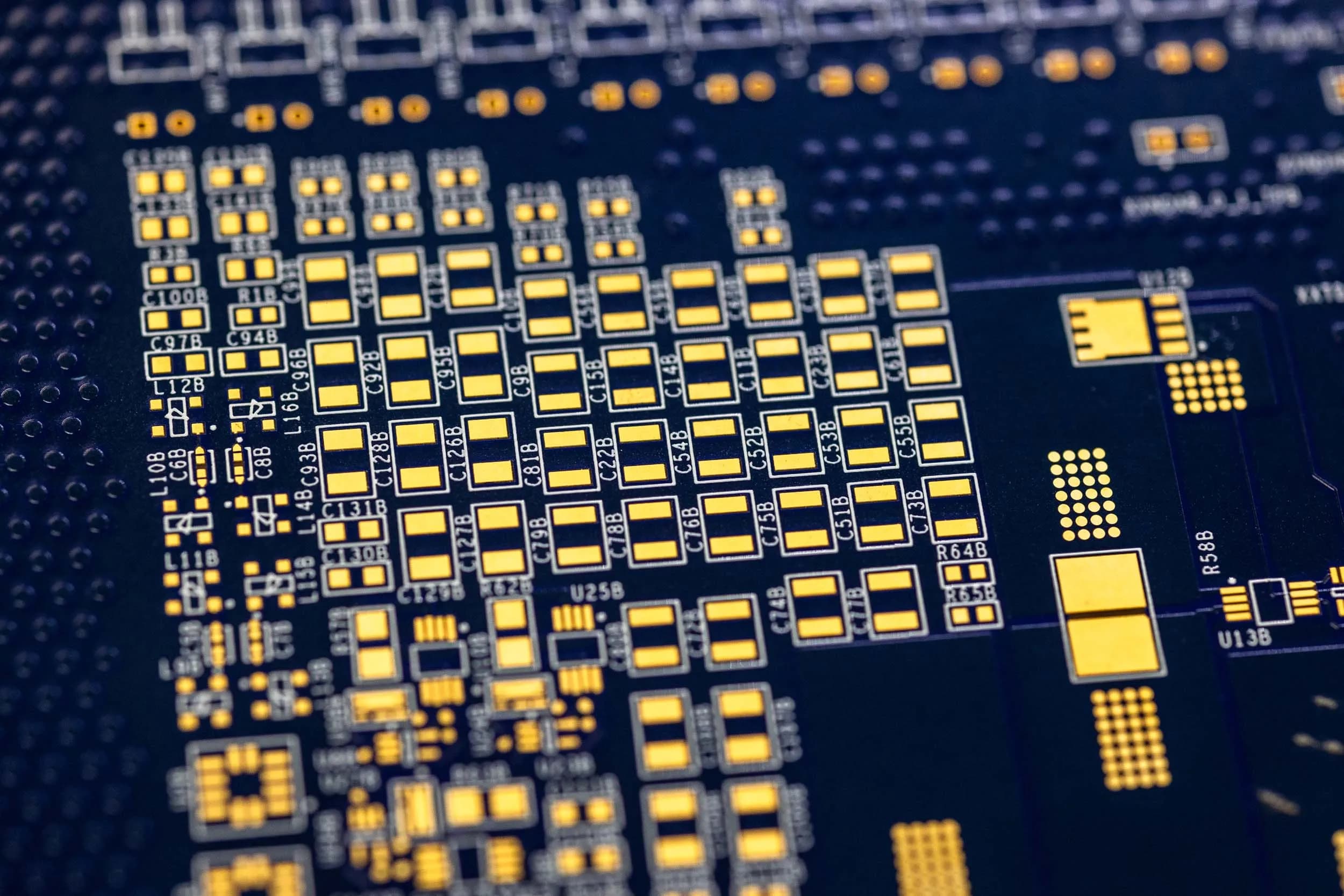
HDI PCB CAPABILITY
High Density Interconnect (HDI) manufacturing supports compact multilayer architectures where routing density and fine-pitch component integration exceed conventional PCB limitations.
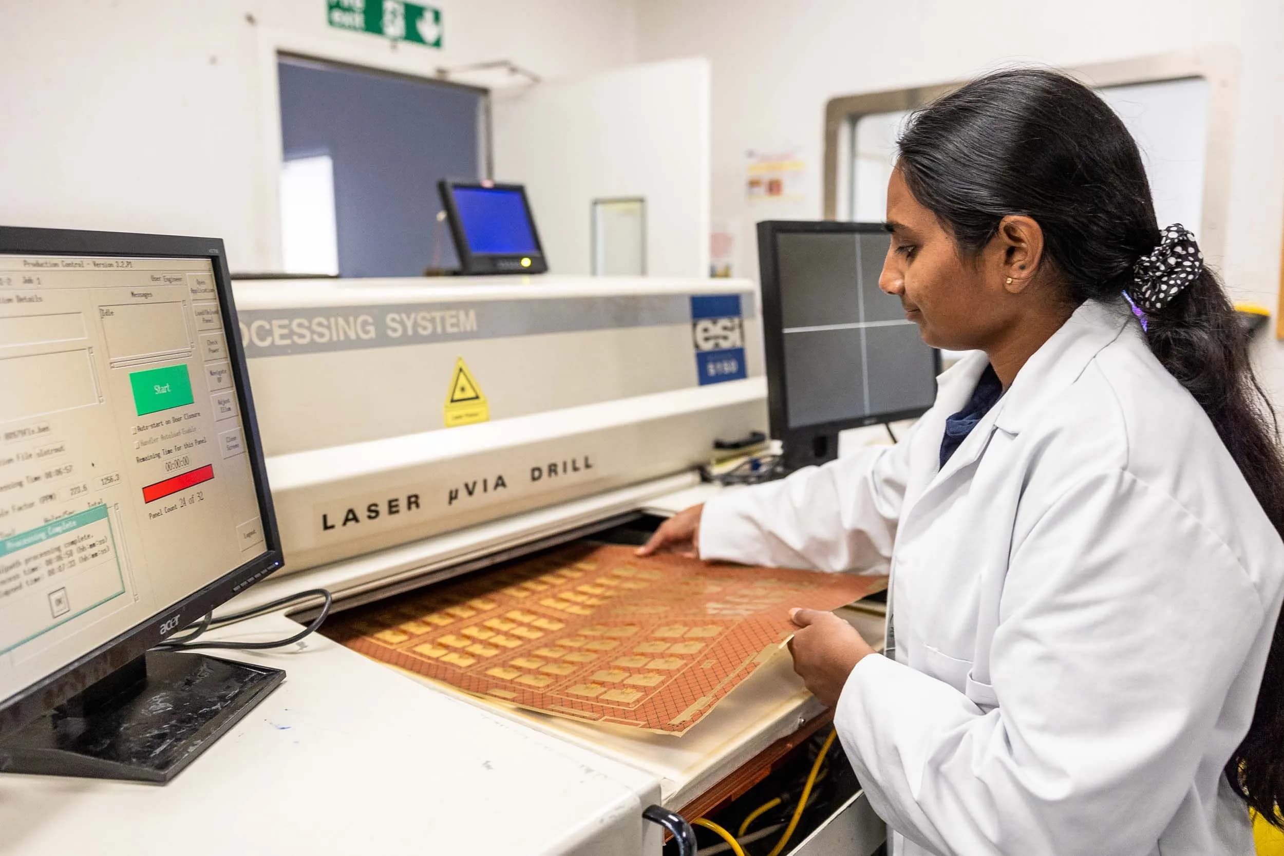
Exception PCB manufactures HDI structures using laser-drilled microvias, sequential lamination, precision registration, and advanced via architectures.
Engineering oversight ensures HDI structures remain manufacturable while maintaining electrical stability and long-term reliability.
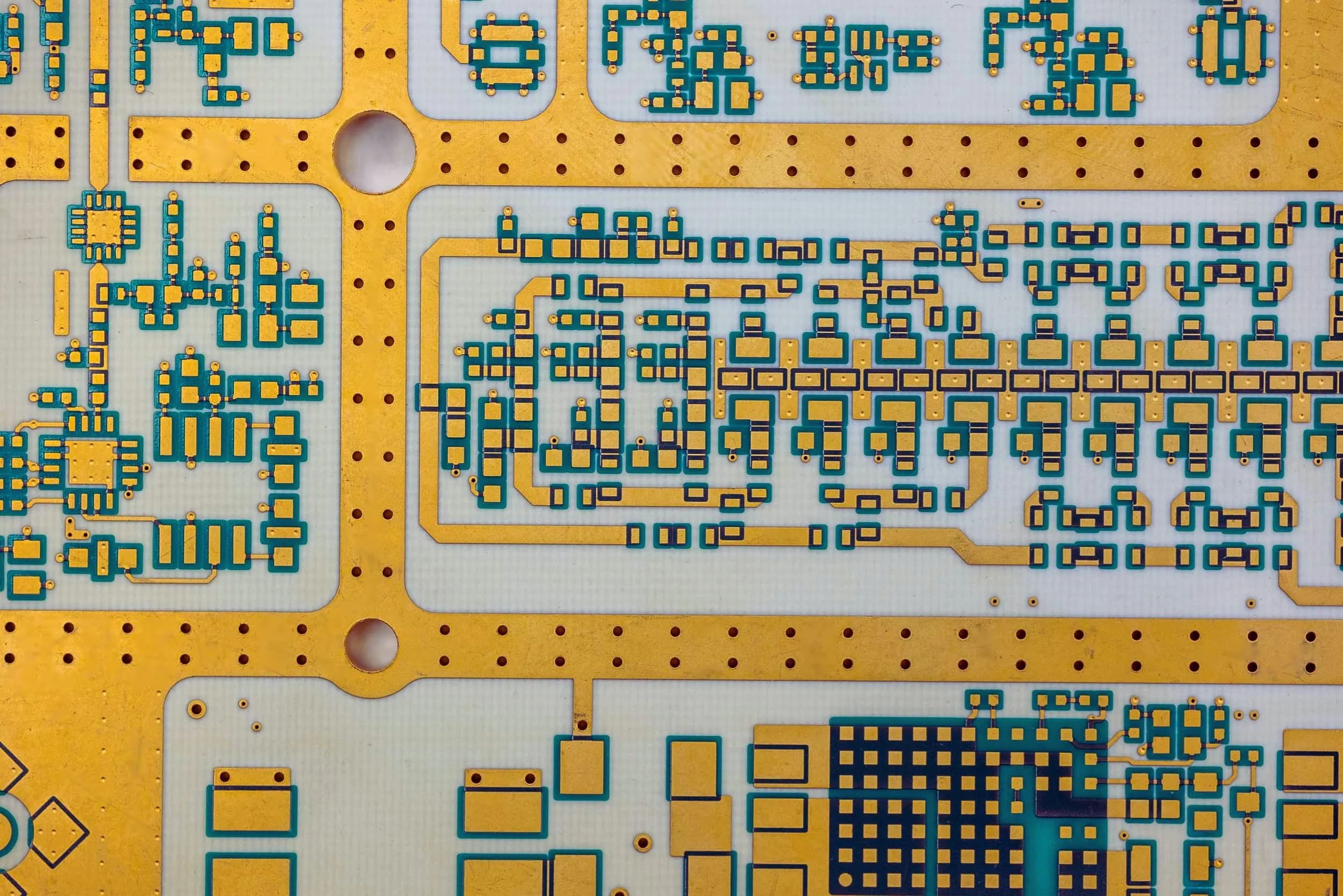
RF PCB CAPABILITY
RF PCB manufacturing requires stable materials, controlled impedance, and precise process control to support predictable high-frequency performance.
Exception PCB manufactures RF and microwave PCB structures using low-loss materials, tightly controlled dielectric thicknesses, and multilayer stack-up engineering designed for signal integrity.
RF capability supports applications where electrical consistency is critical.
ADVANCED PCB MATERIALS
Material selection directly affects electrical performance, thermal behaviour, and manufacturability.
Exception PCB supports a wide range of advanced PCB materials, including FR4 variants, polyimide, PTFE, and hybrid RF constructions.
Engineering guidance helps ensure material systems remain aligned with stack-up architecture and production stability.
COPPER VIA FILL
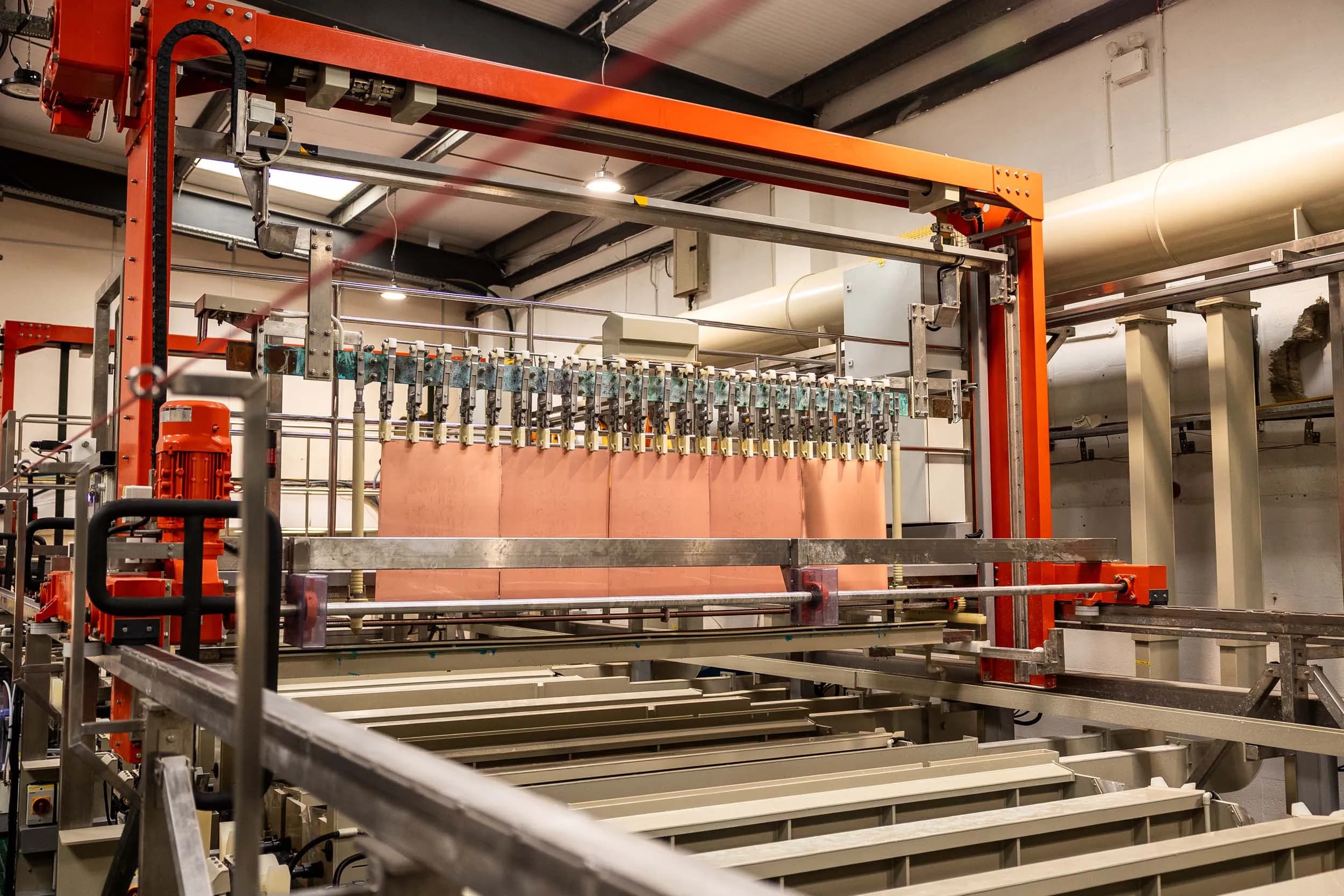
Copper via filling supports dense multilayer designs where thermal conductivity, structural integrity, and via-in-pad architectures are required.
Exception PCB manufactures copper-filled vias using controlled plating processes that promote consistent deposition and stable interconnect performance.
Integrated inspection and microsection validation help ensure via integrity throughout manufacture.
RESIN VIA FILL
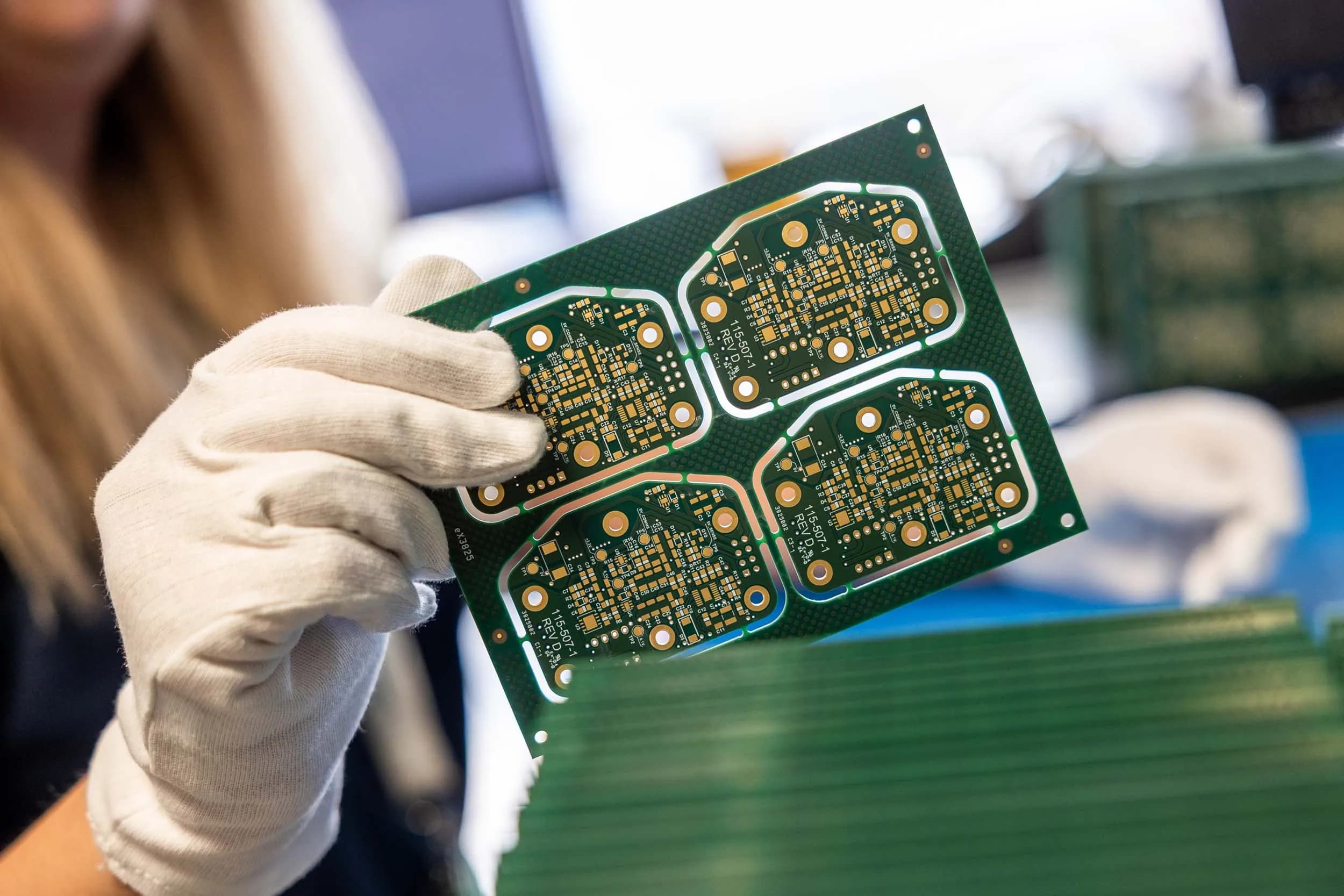
Resin via filling provides planar surfaces for assembly-critical PCB designs where open vias may affect soldering, routing density, or structural stability.
Exception PCB integrates resin via filling within a controlled drilling, filling, curing, and planarisation process to support reliable multilayer construction.
Engineering review ensures filled via structures remain compatible with downstream assembly and long-term reliability requirements.
DOWNLOAD OUR PCB CAPABILITIES
Our capabilities list covers build parameters, tolerances, surface finishes, and drilling specifications across all PCB construction types. Download it to check your design requirements or prepare for a DFM review.
Ready to discuss your project?
Early engagement helps reduce risk and improve outcomes. Whether you are at concept stage, preparing for validation, or planning manufacture, our engineers are available to discuss requirements and offer practical guidance.