
PCB Technical Capabilities
A practical guide to our PCB manufacturing capabilities, tolerances, materials, and processes. Use it to qualify Exception PCB as a supplier, review design requirements, and prepare projects for manufacture.
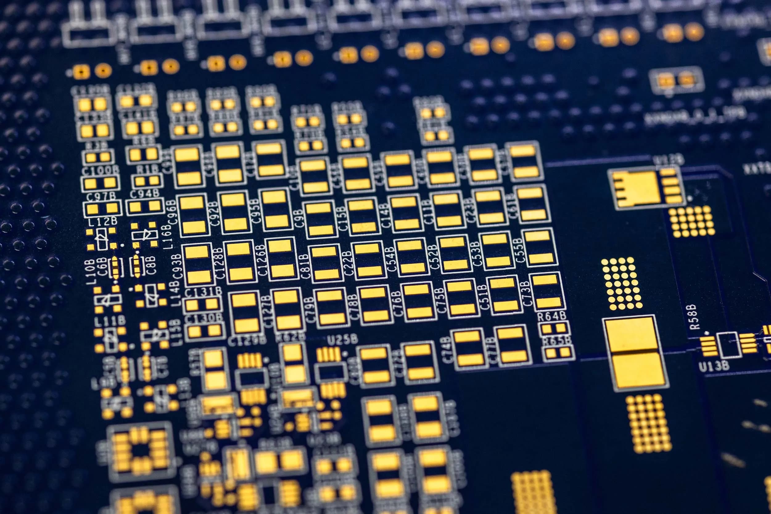
Engineering-led HDI PCB manufacturing from our UK facility, supporting compact multilayer designs where routing density, microvia reliability, and process control are critical.
HDI PCB manufacturing supports designs where routing density, package miniaturisation, and electrical performance exceed what conventional multilayer construction can achieve. At Exception PCB, HDI capability is built around controlled laser drilling, copper via filling, sequential lamination, and precision registration.
HDI manufacture demands tighter dimensional control than conventional PCB fabrication. Our engineers review stack-up design, via strategy, and material selection before production begins, ensuring registration accuracy, dielectric consistency, and microvia quality are maintained throughout
Find answers on microvia dimensions, layer counts, stack-up structures, and process tolerances.
The following capability ranges summarise the HDI manufacturing infrastructure available within Exception PCB’s production environment.
| CAPABILITY | ADVANCED CAPABILITY |
|---|---|
| Maximum layer count | Up to 32 layers |
| Laser microvia diameter | Down to 75 µm |
| Mechanical drill diameter | Down to 0.105 mm |
| Track / gap capability | Down to 50 µm |
| Microvia aspect ratio | Up to 1:1 |
| Sequential lamination | Up to 6 lamination cycles |
| Via structures supported | Blind, buried, stacked, staggered |
| Via filling capability | Copper-filled and resin-filled vias |
| Controlled impedance | ±10% standard / ±5% advanced |
| Electrical testing | 100% electrical test |
These capabilities support compact multilayer PCB architectures where routing density, fine-pitch assembly, and interconnect reliability must coexist within tight dimensional tolerances.
Our engineers review that via geometry, stack-up structure and dielectric selection remain within stable manufacturing limits.
READY TO DISCUSS YOUR HDI DESIGN?
Our engineers can review your stack-up, microvia strategy, and layer requirements, from first prototype through to production.
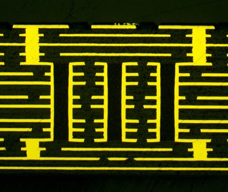
Cross-section of HDI microvia structures showing copper layer interconnection and via geometry within a multilayer PCB build.
Microvia quality is critical to HDI reliability.
Exception PCB manufactures HDI structures using precision laser drilling systems designed to produce consistent via geometry and accurate layer registration.
LASER-DRILLED MICROVIAS SUPPORT:
Microvia geometry is controlled to ensure reliable plating performance and compatibility with sequential lamination processes.
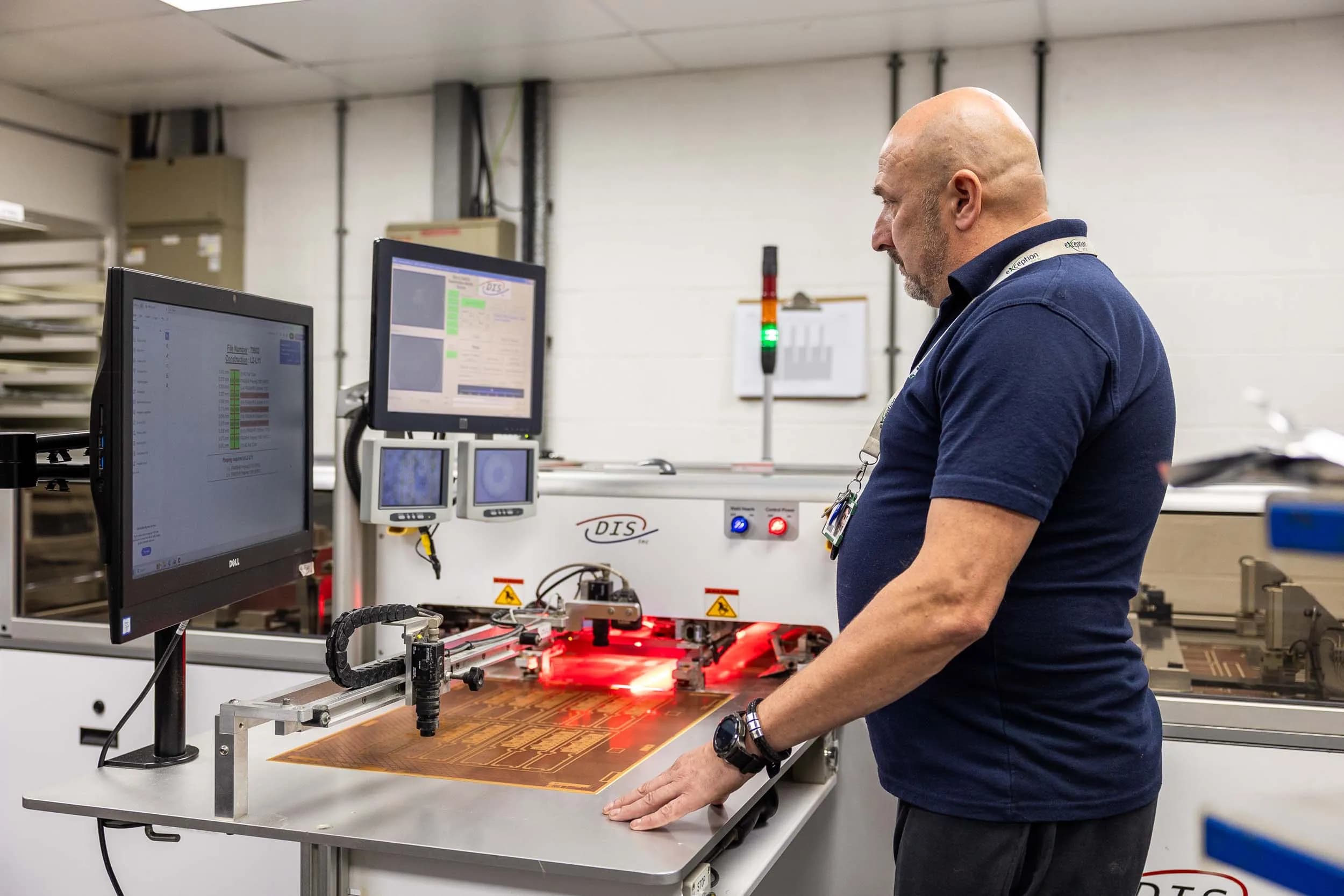
HDI PCB designs frequently require multiple lamination cycles to support layered via constructions.
Exception PCB supports multi-bond lamination processes that allow complex stack-ups to be manufactured with stable registration and controlled dielectric thickness.
SEQUENTIAL LAMINATION ENABLES:
Each lamination cycle is controlled to minimise movement between layers and maintain registration accuracy across the finished build.
HDI reliability depends heavily on via architecture and plating consistency. Exception PCB supports multiple via structures depending on design intent.
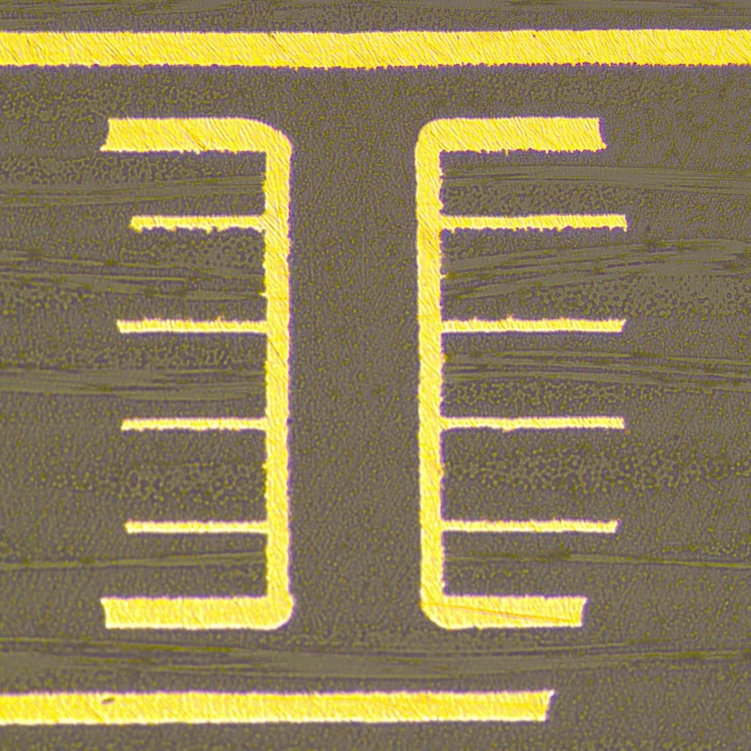
On a HDI design blind vias connect outer layers to inner layers. These are filled with copper or resin to create a planar surface that supports via-in-pad. Using blind vias enables high density component placement.
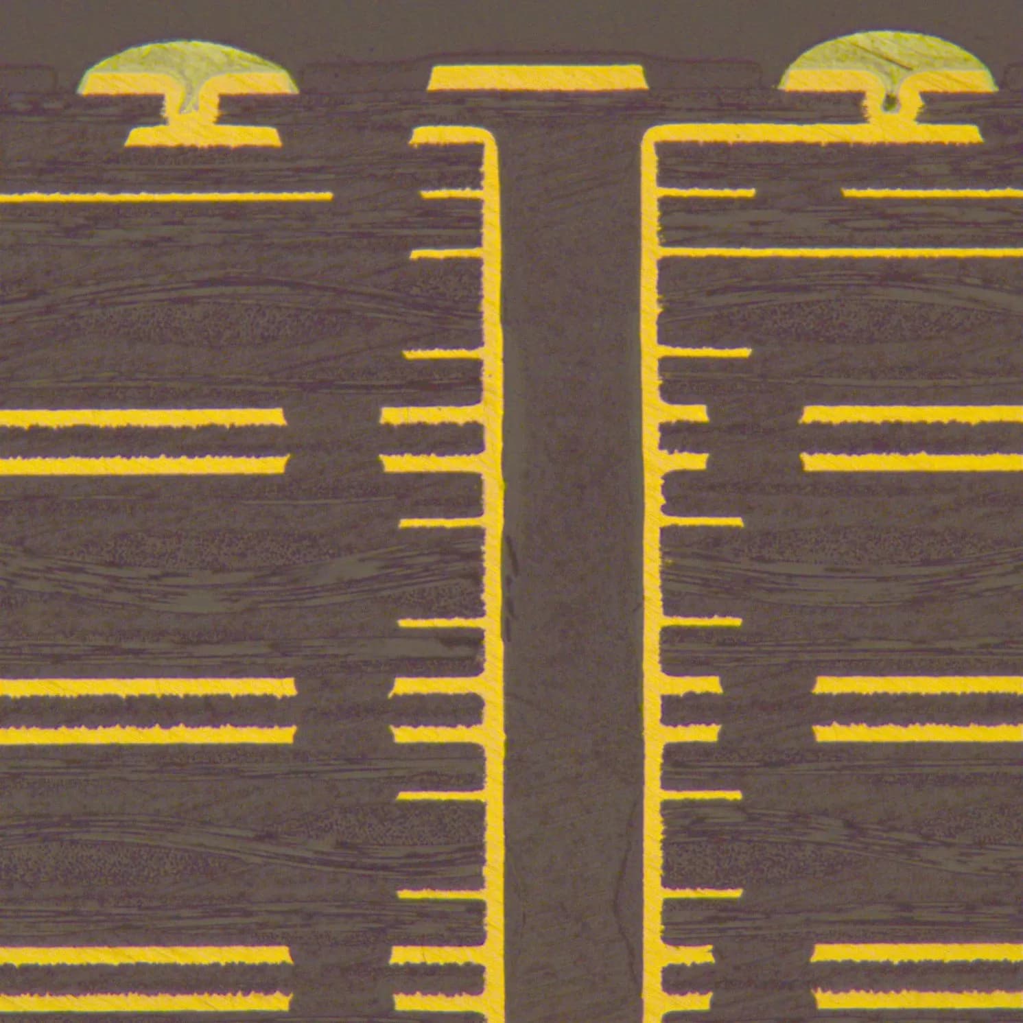
Buried vias create 3-dimensional interconnections in HDI boards. They are located between internal layers and are filled prior to the final lamination stages. Utilising buried vias supports higher routing density by freeing outer layer space.
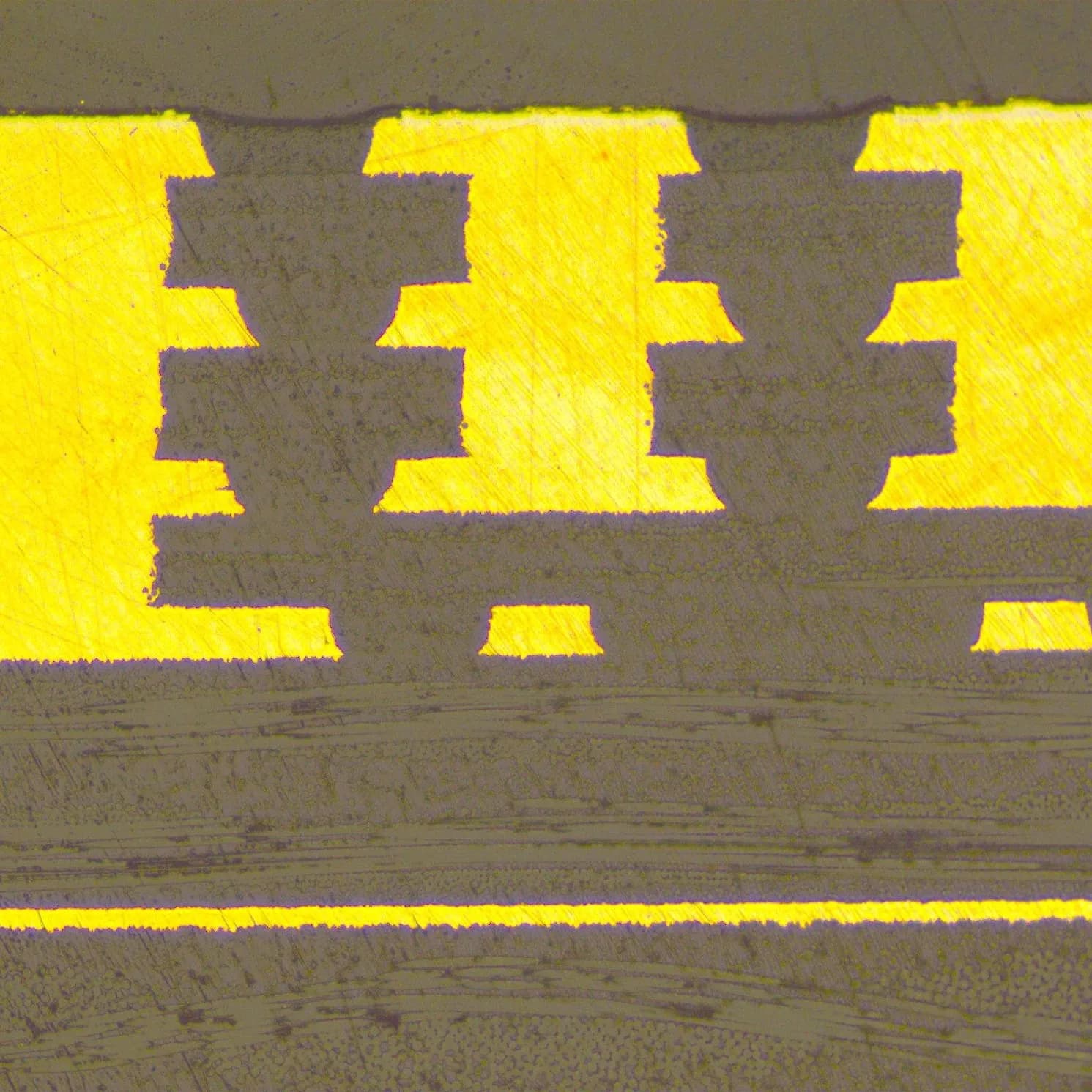
A stacked via design has multiple stages of laser drilling stacked directly on top of each other. These provide vertical interconnection across multiple layers where routing density is very high.
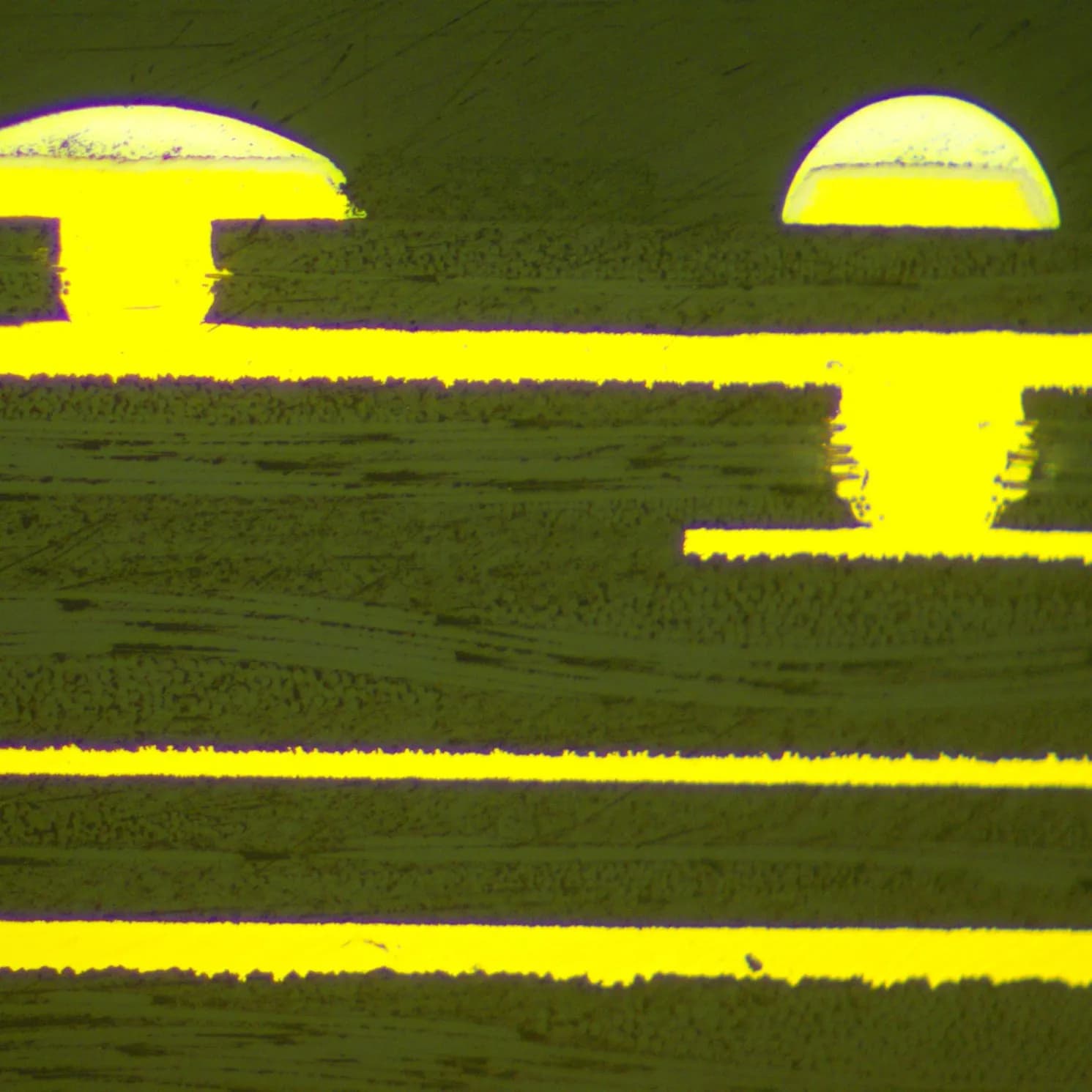
A staggered via is offset from the via below to help improve long term reliability by distributing mechanical stress across the stack-up. This provides a more robust design than using stacked vias.
HDI manufacturing requires stable dielectric materials that maintain dimensional consistency through drilling, lamination, and plating.
Exception PCB supports HDI designs using:
Selecting the right material system is critical to achieving consistent impedance performance, registration stability, and long-term reliability across the full build sequence.
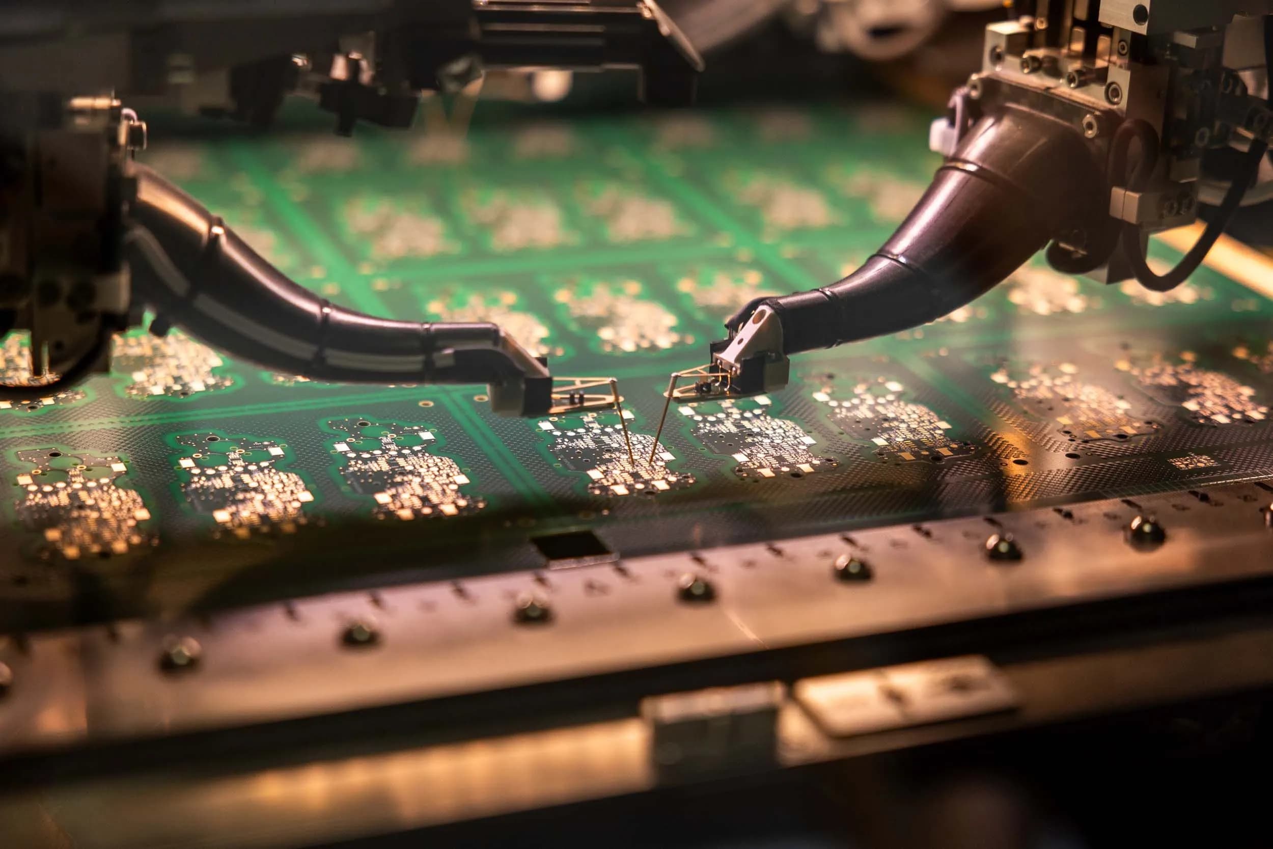
HDI constructions frequently support high-speed digital and RF routing where impedance control becomes critical.
Exception PCB integrates impedance control within HDI stack-up planning to support predictable electrical performance.
CONTROLLED IMPEDANCE BUILDS CONSIDER:
Our engineers us modelling to help ensure impedance targets remain achievable within manufacturing tolerance.
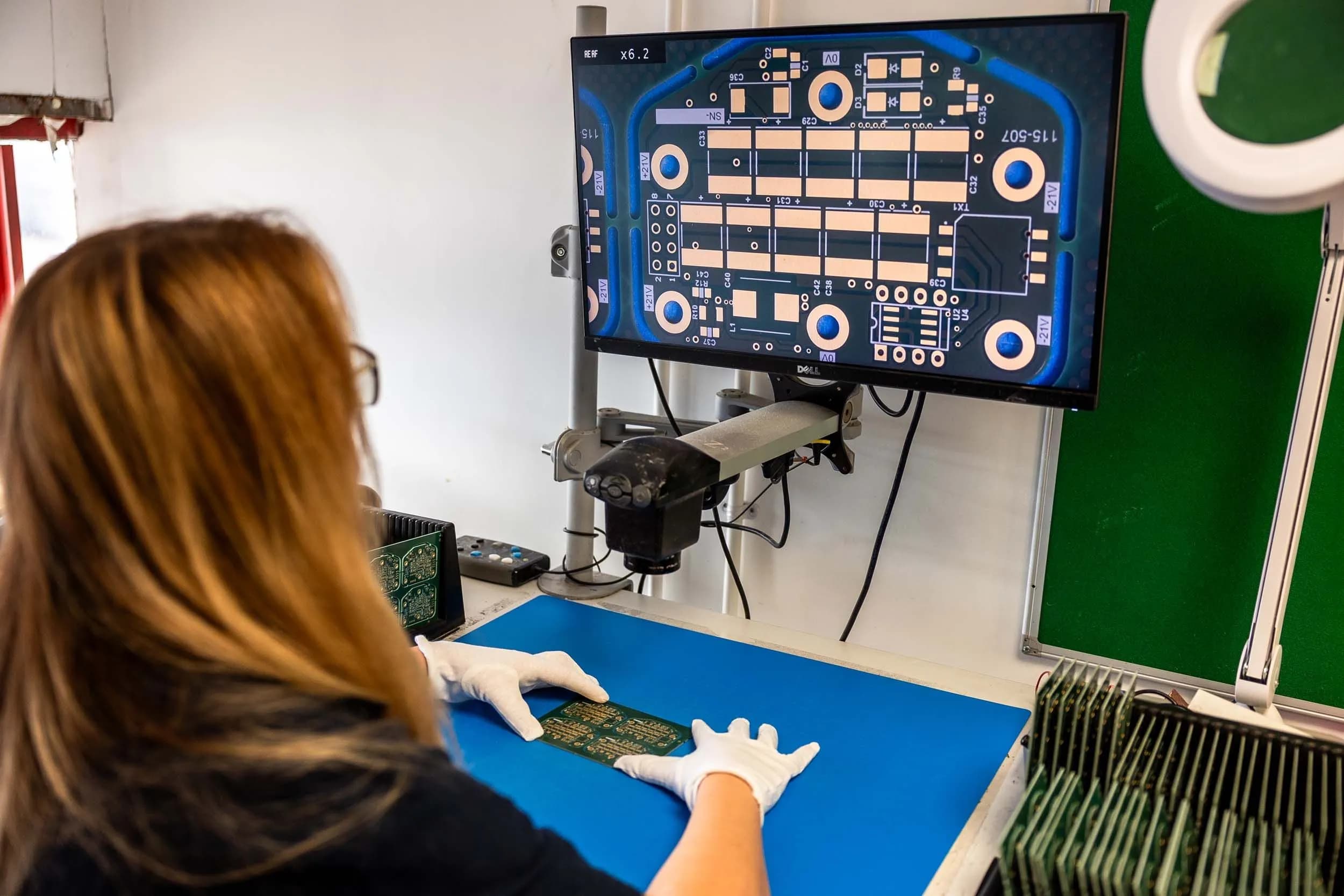
HDI manufacturing requires higher inspection discipline due to reduced feature sizes and increased interconnect density.
Exception PCB integrates verification throughout manufacturing processes to confirm structural integrity, dimensional control and conformance to customer’s design.
INSPECTION INCLUDES:
HDI structures reduce via sizes, increase routing density, and allow for tighter component placement, making them well suited to systems where size, weight, and electrical performance must be balanced within a constrained footprint.
AEROSPACE & DEFENCE ELECTRONICS
Avionics and defence systems demand HDI constructions that meet tight impedance tolerances, full manufacturing traceability, and qualification standards including IPC Class 3. Layer counts of 16 or more with sequential lamination cycles are common, and consistent process control across every build is non-negotiable.
RF AND MICROWAVE SYSTEMS
HDI enables shorter signal paths and reduced parasitic inductance, both of which matter at RF and microwave frequencies. Laser-drilled microvias allow signal routing to remain tight to active components, supporting controlled impedance continuity from component pad to interconnect.
MEDICAL INSTRUMENTATION
Miniaturised medical devices use HDI to accommodate fine-pitch components and dense routing within constrained form factors. Manufacturing consistency and the ability to build complex stack-ups repeatably are as important as the initial design specification.
HIGH-SPEED PROCESSING HARDWARE
Processors, FPGAs, and memory interfaces operating at multi-gigabit speeds place high demands on signal integrity. HDI construction reduces stub lengths, supports back-drilling where required, and allows differential pairs to be routed with the consistency these data rates demand.
Our engineers work with customers from early design through to manufacture, ensuring HDI constructions are both buildable and optimised for the manufacturing process.
Many of the issues that cause delays or re-spins in HDI programmes originate at the design stage, and early engineering input is the most effective way to address them.
OUR ENGINEERS REGULARLY REVIEW:
TALK TO OUR ENGINEERS
Whether you are working on a HDI project, or planning a complex multilayer design, our engineering team can support the right manufacturing approach.
Below we have answered the questions our engineers are asked most often. If yours isn't covered, get in touch with the team directly.
HDI PCBs typically incorporate blind or buried vias, fine-line routing, and sequential lamination.
The objective is to increase routing density while maintaining or reducing overall board size.
HDI DESIGNS OFTEN SUPPORT:
Laser vias are used to reduce the space consumed by traditional mechanical through vias.
They allow interconnections between adjacent layers without routing through the full board thickness.
THIS IMPROVES:
Yes. HDI designs frequently require impedance-controlled routing for digital and RF applications.
CONTROLLED IMPEDANCE IS ACHIEVED THROUGH:
Sequential lamination is a manufacturing process where the PCB is built using multiple lamination stages. It is commonly used for HDI designs allowing the use of buried and blind vias.
Additional layers and vias are built progressively and added to the top and bottom of the stack at each stage, enabling the creation of complex HDI interconnections.
Explore guides and references covering PCB construction types, material selection, and the full range of capabilities available at Exception PCB.
Explore related technologies that support dense HDI structures, including via filling, material selection, compact constructions and controlled electrical performance.
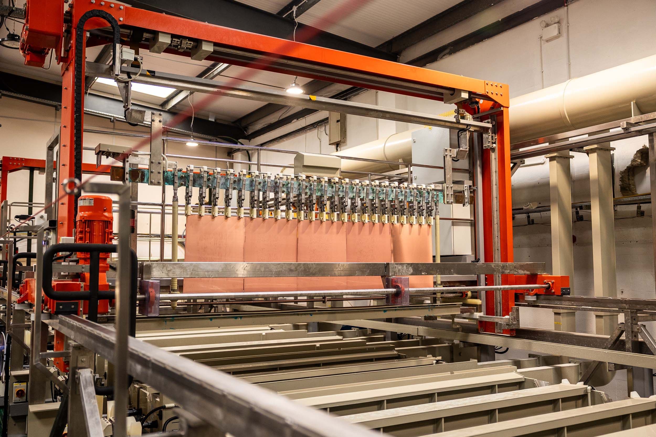
Copper via filling for blind, buried, and through-hole vias, supporting HDI constructions, via-in-pad designs, and thermally demanding multilayer PCBs where electrical continuity, thermal performance, and consistent fill quality are required.
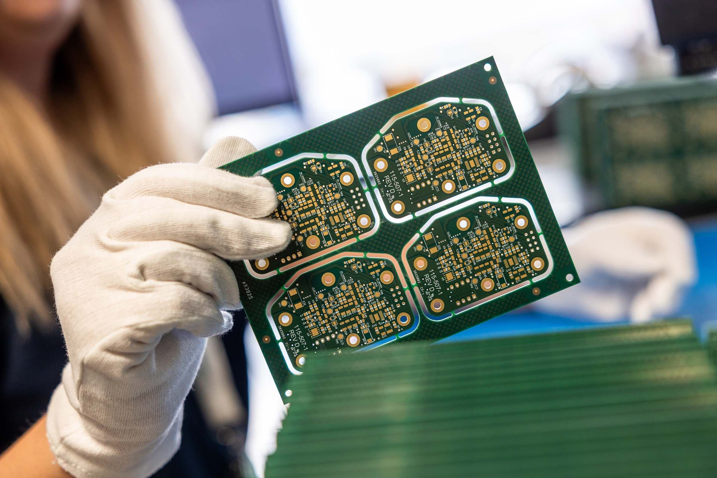
Resin via fill for blind, buried, and through-hole vias, providing consistent surface planarity to support via-in-pad designs, fine-pitch assembly, and sequential lamination builds where assembly quality and via integrity matter.
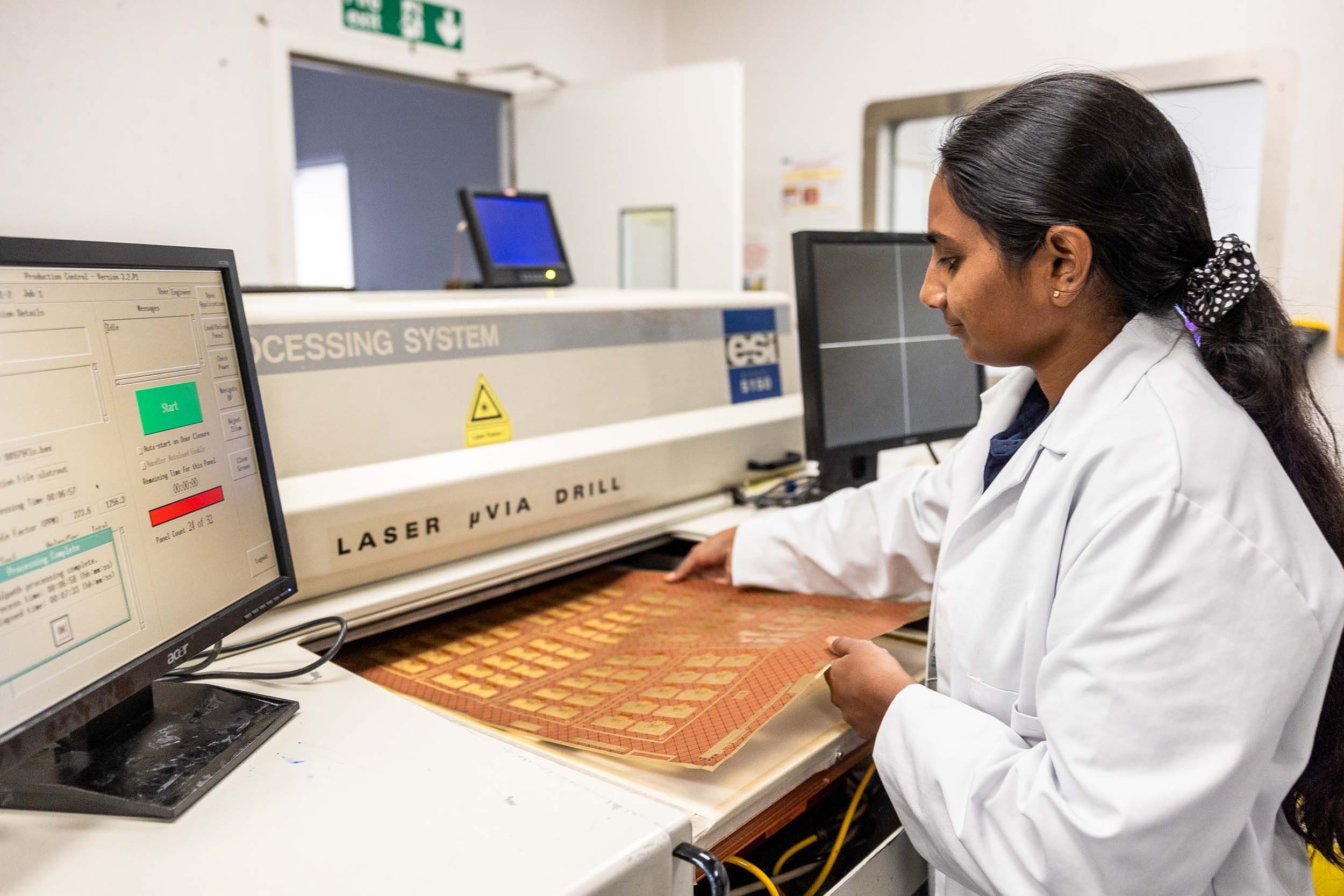
Support for specialist and hybrid PCB materials selected to meet thermal, electrical, and environmental performance requirements in applications where standard FR4 or conventional laminate systems cannot deliver the required performance.
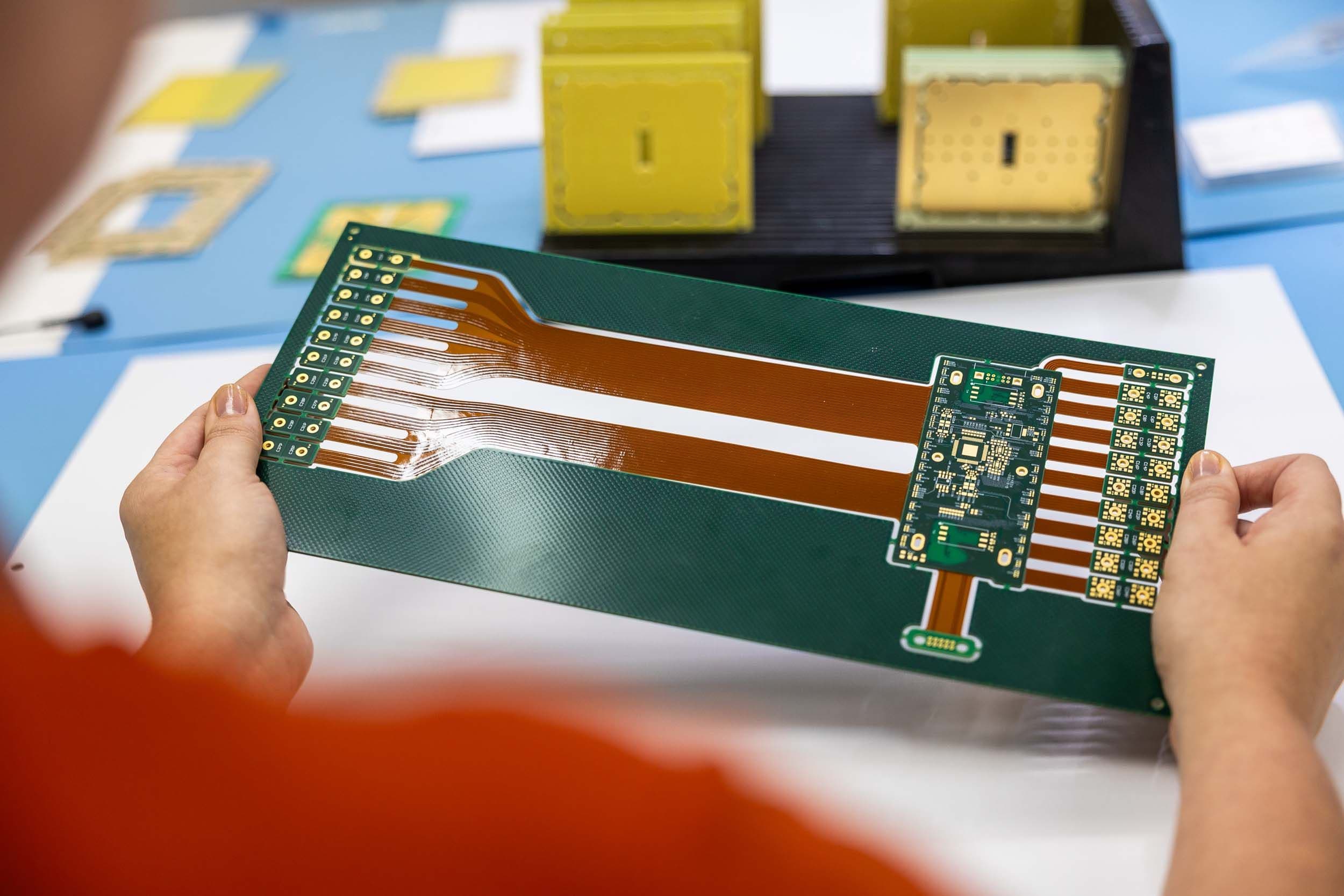
Complex flex and rigid-flex PCB constructions for space-constrained and dynamic applications, built with reliability and repeatability in mind to support confident integration where weight, form factor, or movement are critical.
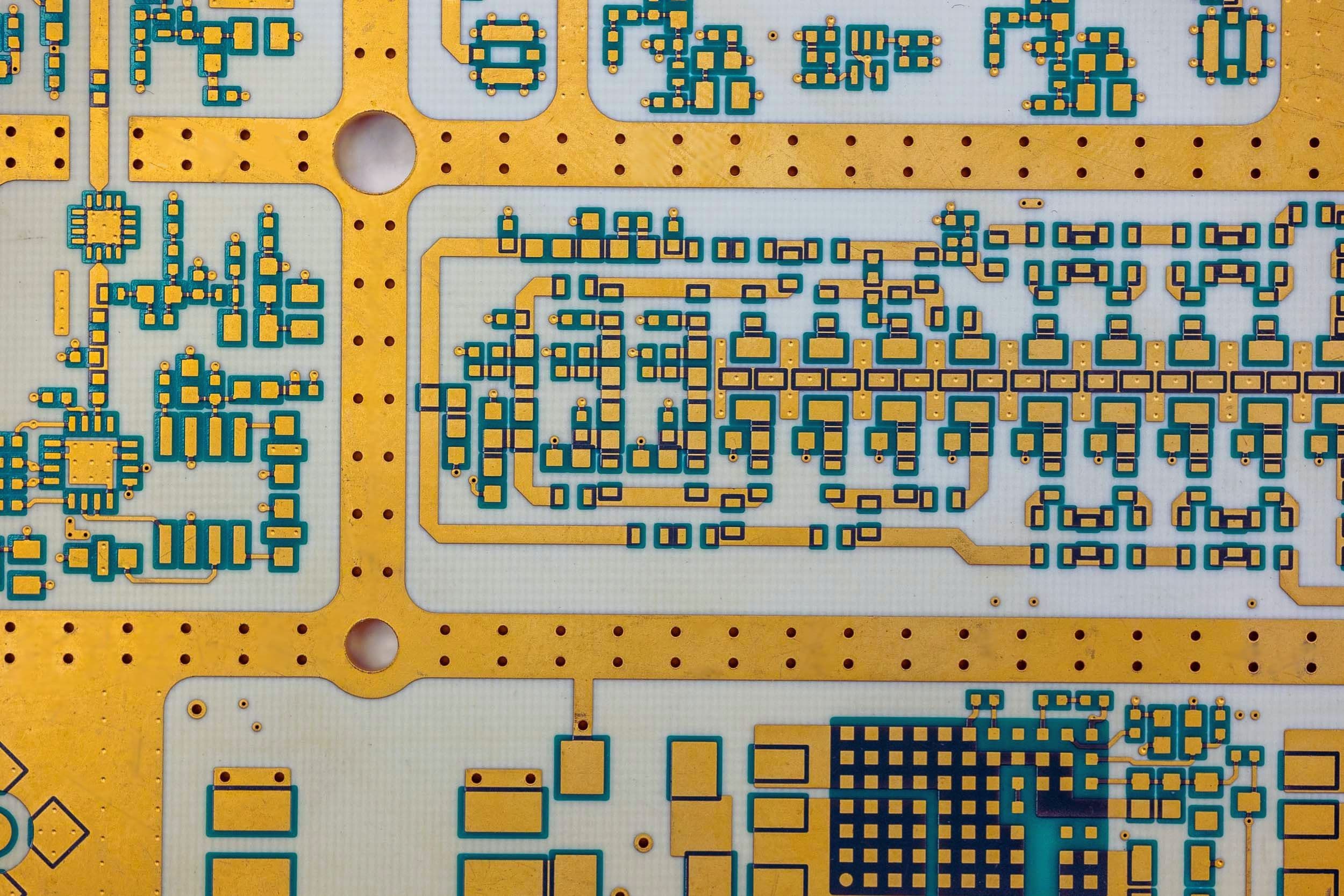
RF and high-frequency PCBs built to support controlled impedance, low-loss materials, and consistent signal integrity in demanding applications where dielectric performance, layer registration, and material choice directly affect circuit behaviour.