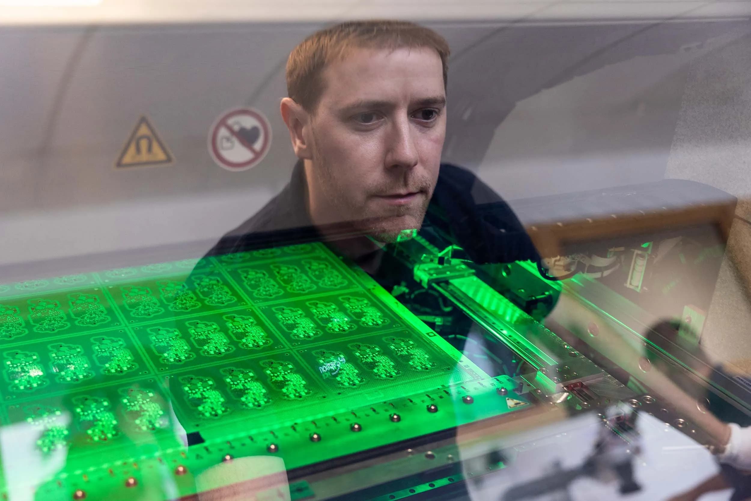
An Exception PCB technician looking through a protective glass window at an illuminated circuit board panel.

PCB PROTOTYPING SERVICES

Engineering-led PCB prototyping from our UK facility, supporting design validation, NPI, and low-volume manufacture to full production standards.

ENGINEERING-LED PCB PROTOTYPING

Prototyping at Exception PCB is engineering-led and built around one purpose: validating designs properly and reducing risk before committing to volume. We support design validation, NPI, and low-volume manufacture for complex and high-technology applications.

We work closely with engineering teams throughout early-stage development, design refinement, and functional testing, providing DFM feedback and build-route guidance drawn from hands-on manufacturing experience. Our prototypes are built to reflect real production conditions, giving your team the information to make confident decisions.

LET OUR ENGINEERS ASSESS YOUR DESIGN FOR MANUFACTURE

Whether you are validating a new concept or preparing for NPI, our team will identify any manufacturability risks and confirm the right prototyping route before your build begins.

Talk to our engineers

PCB PROTOTYPING PROCESS

Every prototype follows the same controlled manufacturing route applied to production builds, with engineering input and inspection integrated throughout.

STAGE 1

ENGINEERING AND CAM REVIEW

Design data is reviewed before fabrication begins. Our engineers assess stack-up, materials, drill structures, impedance, and tolerances, providing DFM feedback and confirming build-route intent.

STAGE 2

INNER LAYER IMAGING AND AOI

Inner layers are produced using precision imaging and etching. Automated optical inspection verifies track definition, spacing, and registration before lamination.

STAGE 3

LAMINATION

Inspected inner layers are laminated under controlled temperature and pressure, ensuring consistent bonding, resin flow, and layer alignment.

STAGE 4

DRILLING AND PLATING

Interconnections are formed through mechanical and laser drilling, followed by automated copper deposition to build conductive paths and via structures.

STAGE 5

OUTER LAYER IMAGING AND AOI

Outer circuitry is defined through imaging and etching, with automated optical inspection confirming pattern integrity and registration.

STAGE 6

ELECTRICAL TEST

All boards undergo 100% electrical testing to verify continuity and isolation across every net.

STAGE 7

FINAL INSPECTION AND DISPATCH

Completed boards are verified, documented, and dispatched with full material and process traceability, supporting confident design progression and follow-on manufacture.

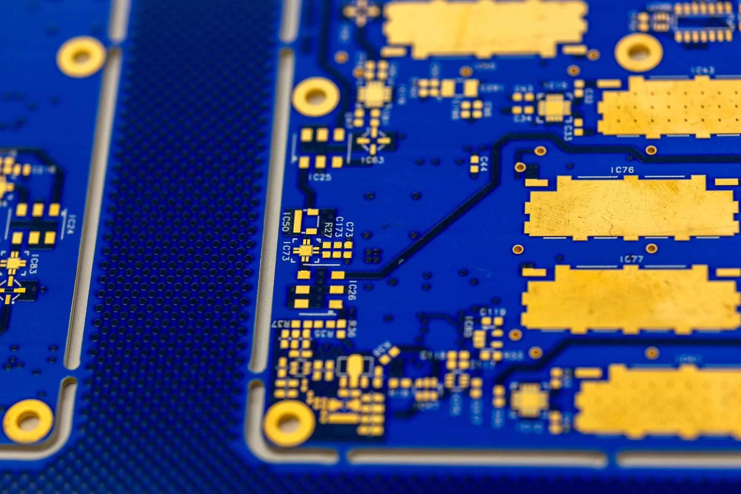
A detailed close-up of a blue printed circuit board showing trace routing and integrated circuit component pads.

PROTOTYPE LEAD TIMES

Prototype lead times are determined by design complexity, materials, and validation requirements. We offer flexible delivery options to suit different programme needs.

  • Standard prototype lead times for complex, production-ready builds
  • Accelerated options available where project timelines require faster delivery

Clear expectations confirmed at quotation stage, with no ambiguity


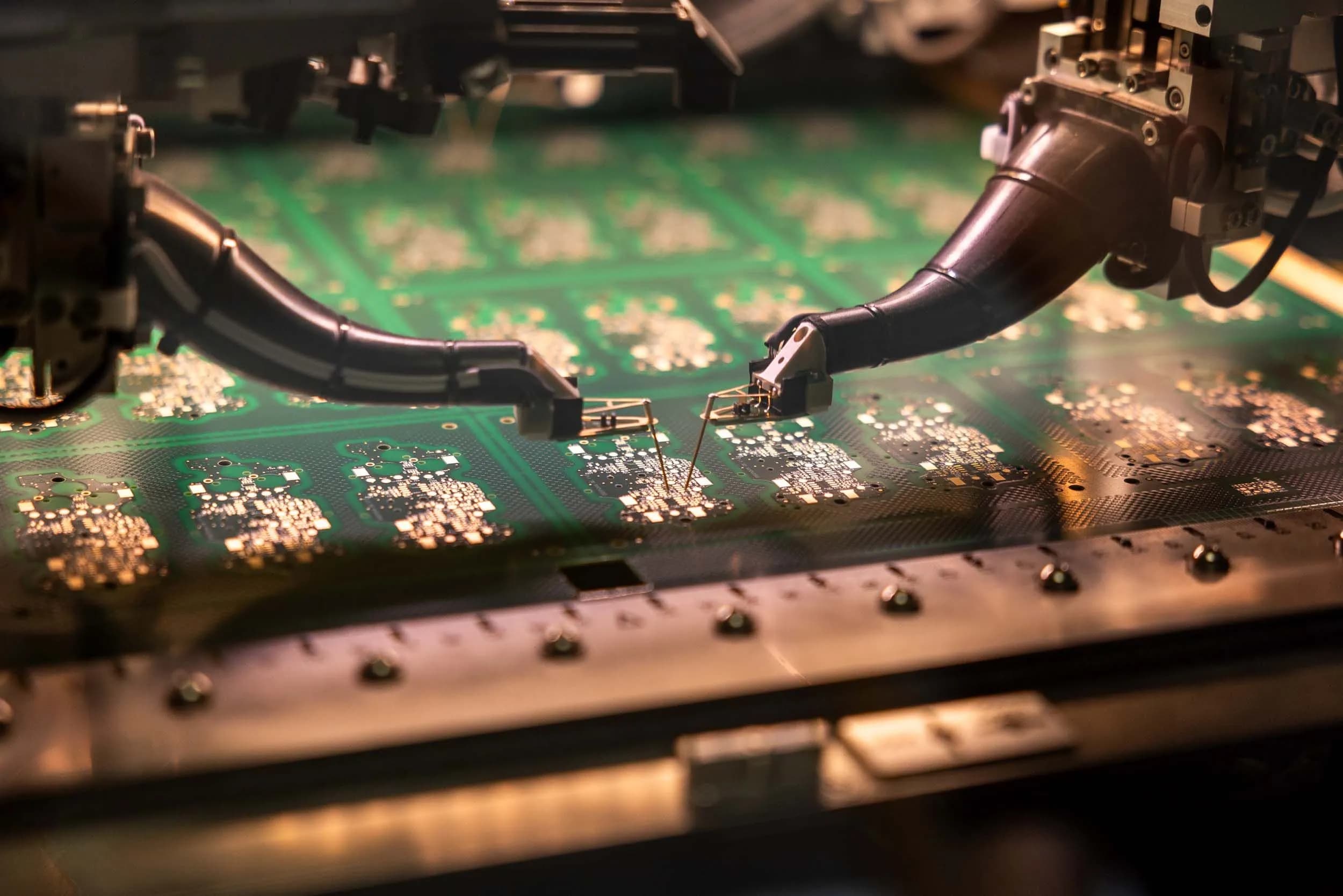
Close-up of flying probe test heads making electrical contact with a multilayer PCB during automated testing at Exception PCB

QUALITY AND ASSURANCE

Quality does not change at prototype stage. Every prototype is manufactured and inspected within our controlled quality environment.

OUR PROTOTYPING SERVICE INCLUDES:

  • AOI on internal and external layers
  • 100% electrical test
  • Microsection analysis where required
  • Full material and process traceability
  • Documentation aligned to regulated-sector expectations

This ensures prototypes provide meaningful data and behave consistently during functional testing and validation.

Learn more about our quality

PCB TECHNOLOGIES FOR PROTOTYPING AND NPI

We support prototypes across a broad range of PCB technologies, including complex constructions that require careful review of materials, stack-up, and manufacturing approach. The pages below provide detailed information on each technology area, including what is achievable at prototype stage and how design choices influence the transition to production.

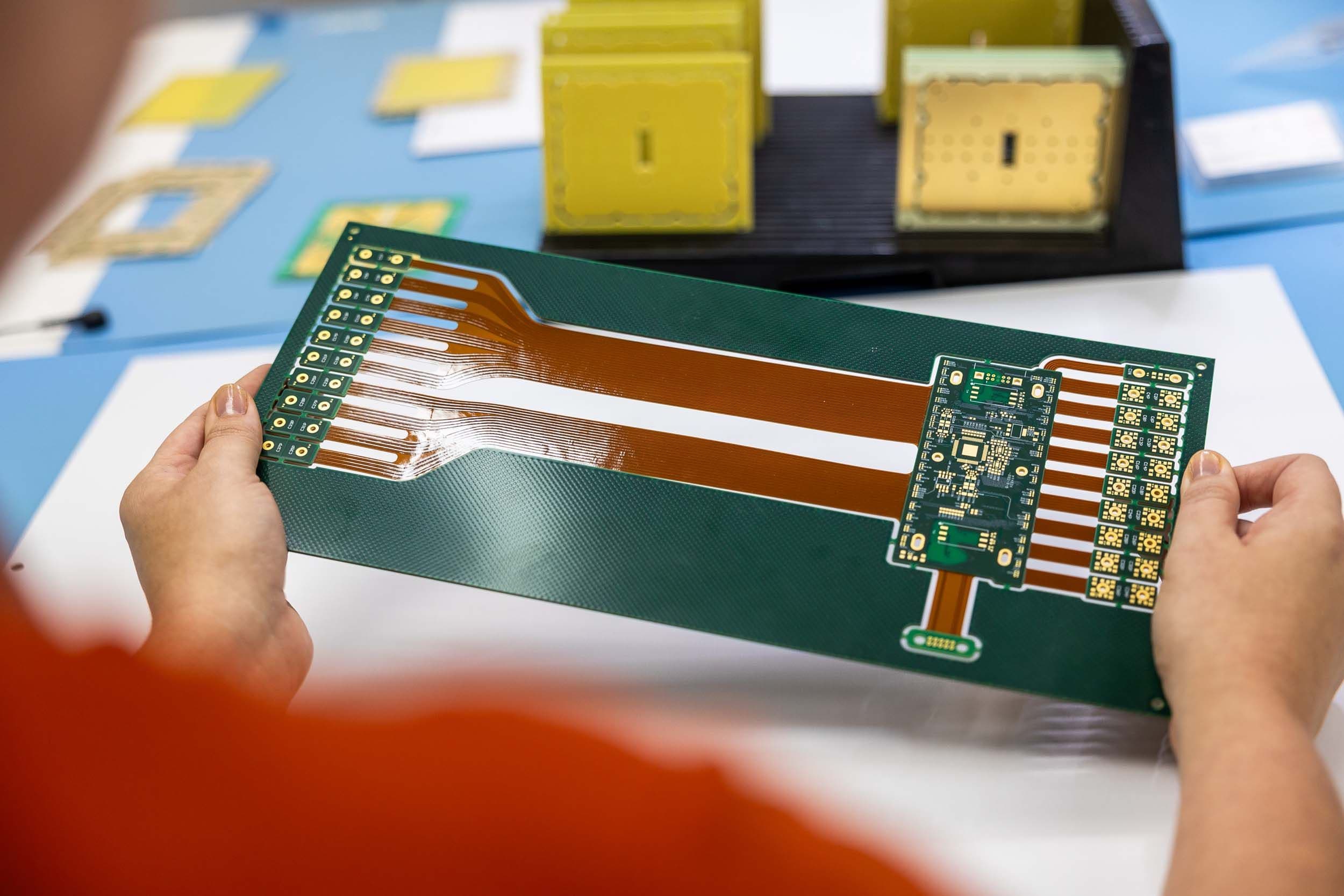
Technician holding a complex green rigid-flex circuit board panel with amber flexible interconnect extensions.

Flex & Rigid-Flex

Complex flex and rigid-flex PCB constructions for space-constrained and dynamic applications, built with reliability and repeatability in mind to support confident integration where weight, form factor, or movement are critical.

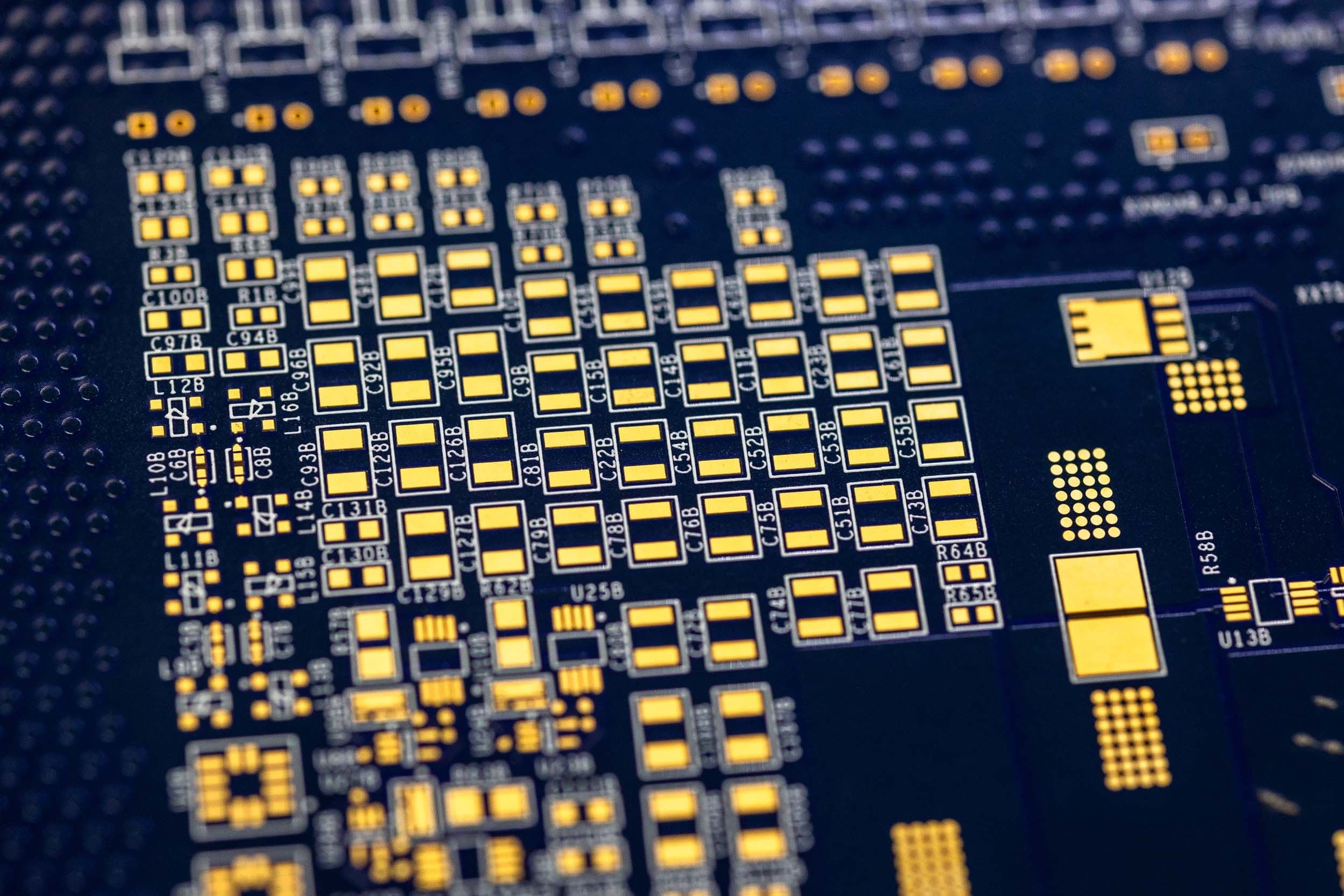
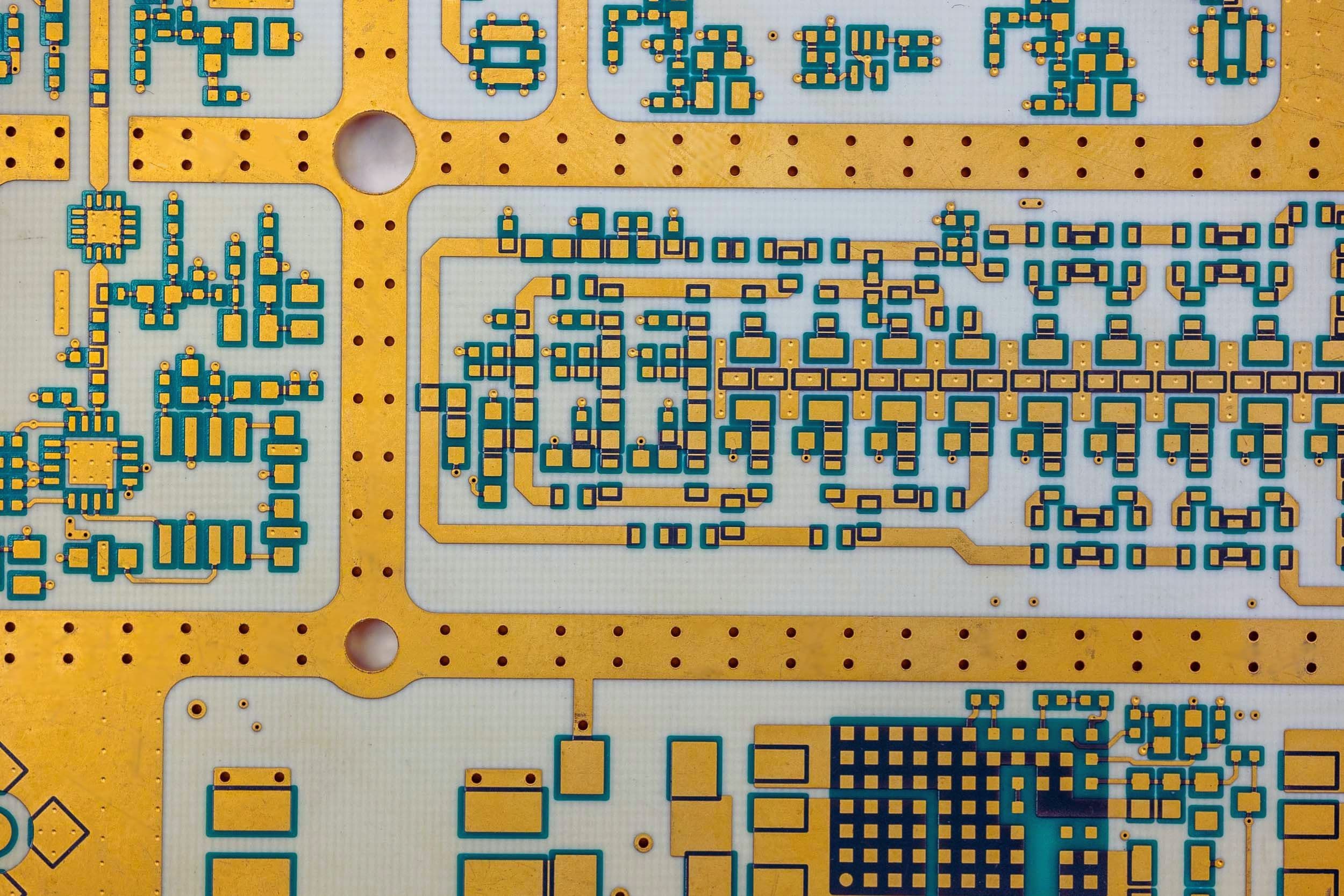
Macro view of a dark, high-density PCB showing precise gold pad layouts and trace routing.

HDI

High-density interconnect PCBs for fine features, microvias, and complex multilayer designs, manufactured using production-ready processes with full engineering oversight to ensure reliable and repeatable fabrication of the most demanding constructions.

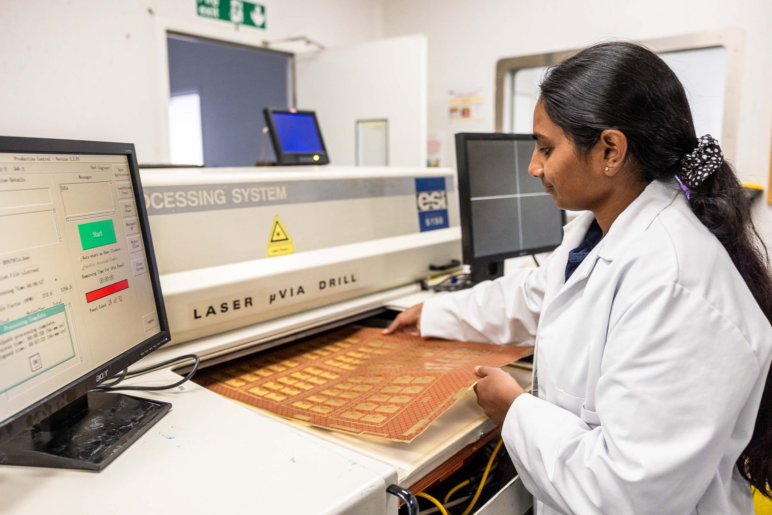
Exception PCB operator loading a flexible printed circuit board panel into an ESI laser micro via drill processing system.

Advanced Materials

Support for specialist and hybrid PCB materials selected to meet thermal, electrical, and environmental performance requirements in applications where standard FR4 or conventional laminate systems cannot deliver the required performance.

Macro close-up of ENIG gold-plated pads and precision circuit trace routing on a white substrate RF PCB, showing the surface finish quality and high-density layout of Exception PCB's RF manufacturing capability.

RF

RF and high-frequency PCBs built to support controlled impedance, low-loss materials, and consistent signal integrity in demanding applications where dielectric performance, layer registration, and material choice directly affect circuit behaviour.

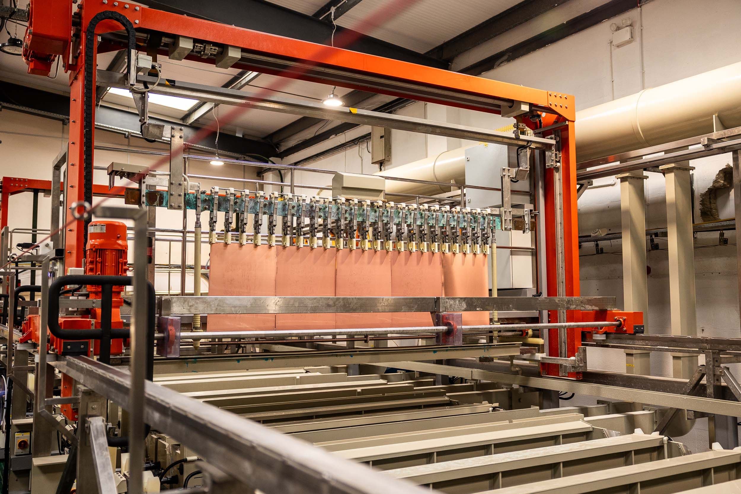
Wide landscape view of an automated electrochemical processing line inside the manufacturing plant.

Copper Via Fill

Copper via filling for blind, buried, and through-hole vias, supporting HDI constructions, via-in-pad designs, and thermally demanding multilayer PCBs where electrical continuity, thermal performance, and consistent fill quality are required.

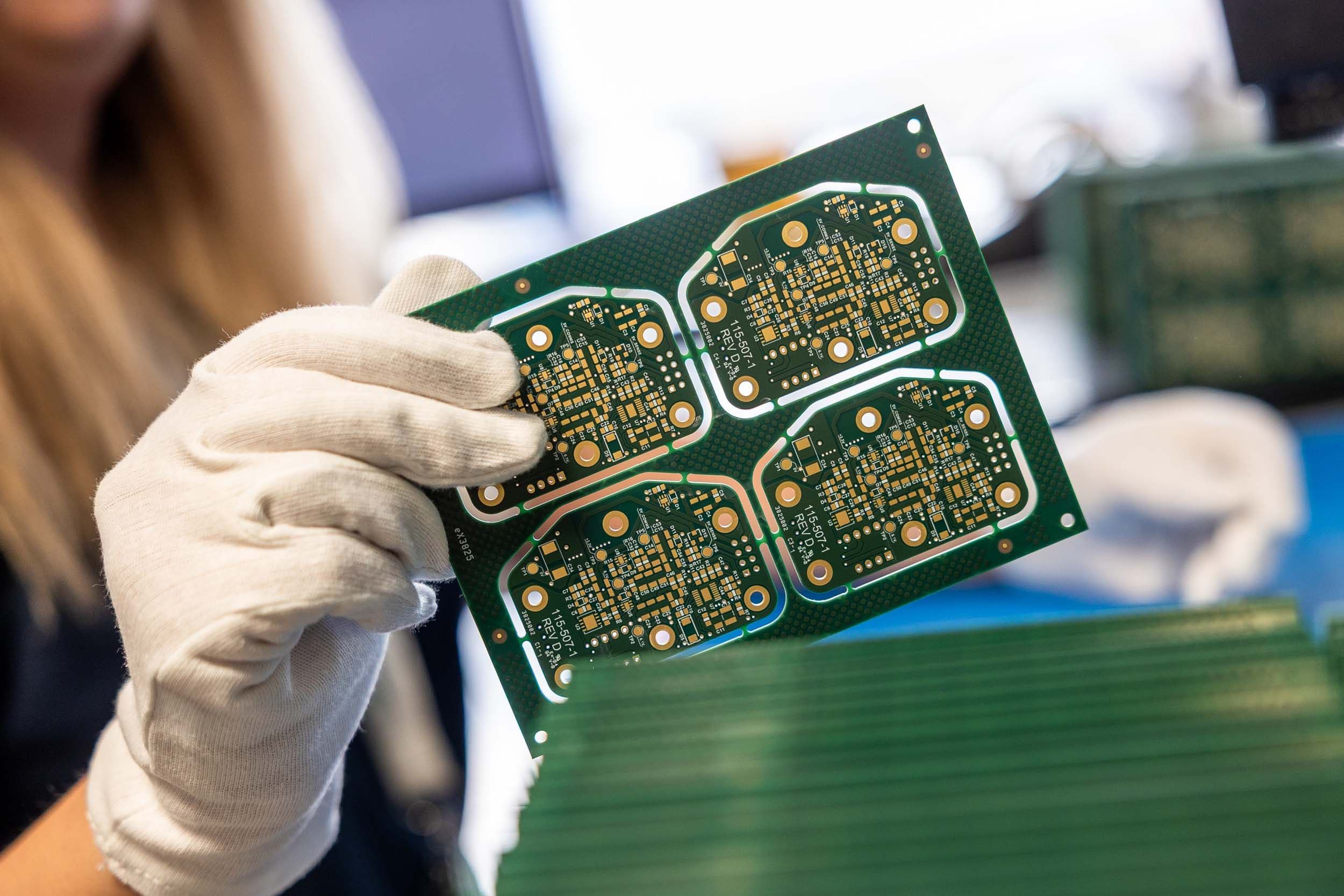
Exception PCB technician in a white glove holding a green printed circuit board panel with four individual circuits.

Resin Via Fill

Resin via fill for blind, buried, and through-hole vias, providing consistent surface planarity to support via-in-pad designs, fine-pitch assembly, and sequential lamination builds where assembly quality and via integrity matter.

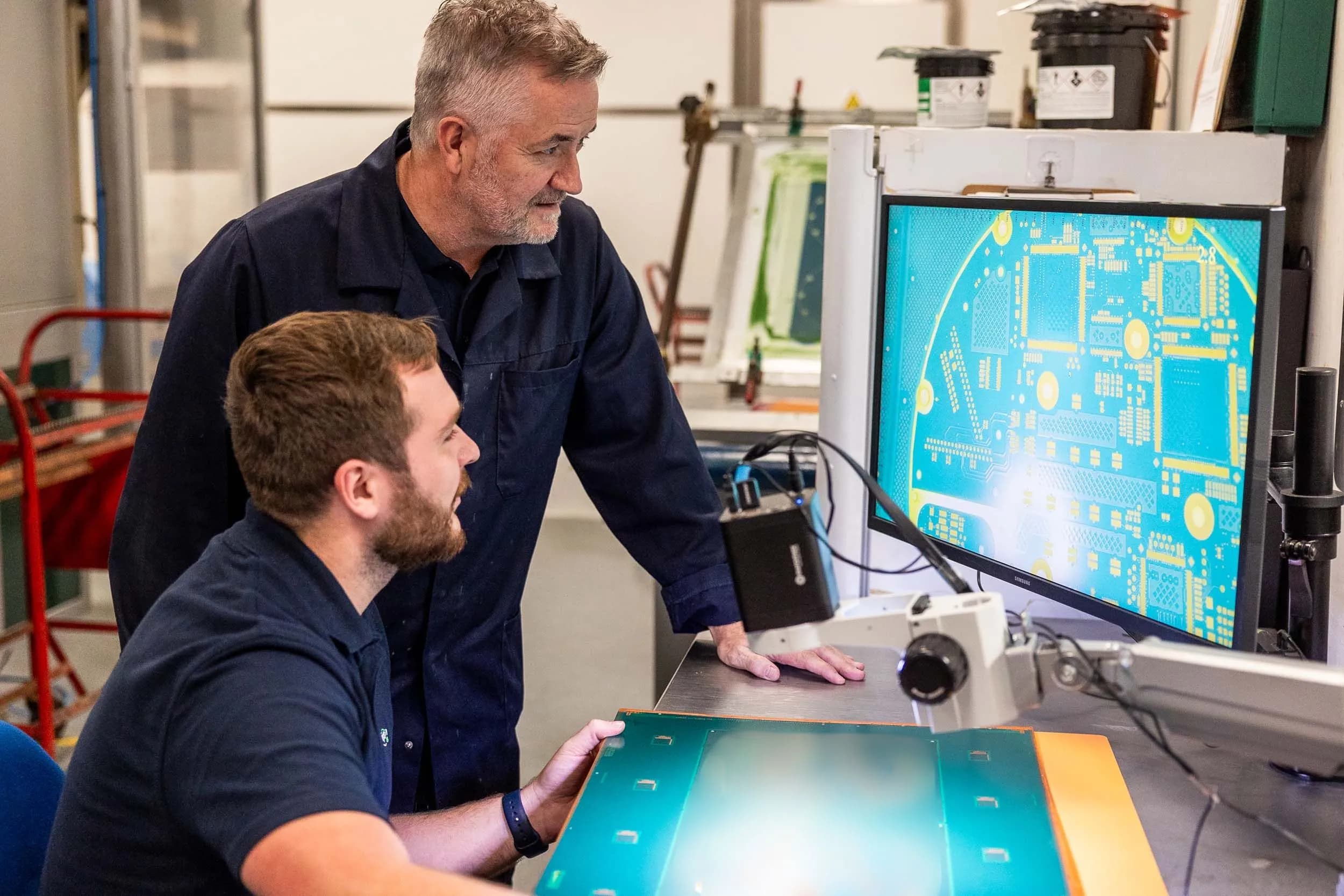
Exception PCB technicians collaborating at a digital microscope inspection workstation.

HOW OUR PROTOTYPING SERVICE SUPPORTS ENGINEERING TEAMS

Engineering teams use our prototyping service to validate designs, confirm performance, and de-risk programmes before scaling.

TYPICAL OUTCOMES INCLUDE:

  • Early identification of layout or stack-up issues
  • Faster iteration between design revisions
  • Greater confidence when transitioning to production
  • Reduced risk of costly re-spins later in the programme

Our role is to support informed engineering decisions, not just deliver a board.

Ready To Discuss Your Project?

If you are developing a new design or preparing for NPI, our engineers are ready to support your prototyping requirements.

RELATED ARTICLES

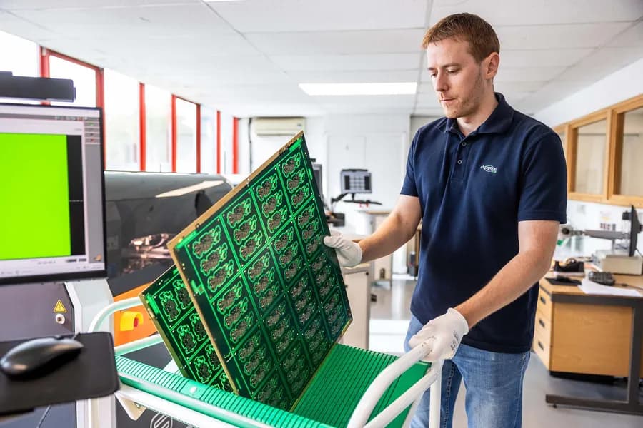
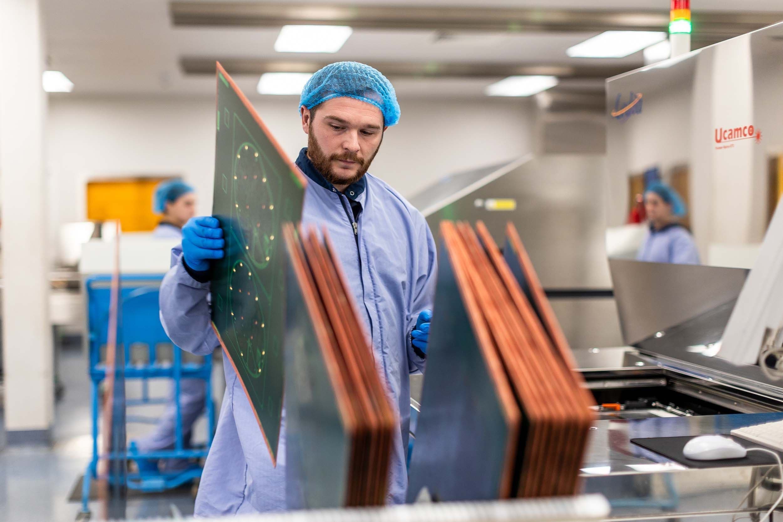
An Exception PCB technician storing green circuit board panels into a protective green slot rack cart.

Why UK Manufacturing Matters for Sovereign Capability

UK-based PCB manufacturing is no longer just a sourcing choice, it is a strategic way to reduce supply chain risk, protect sensitive programmes, improve lead times and strengthen sovereign capability in high-technology electronics.

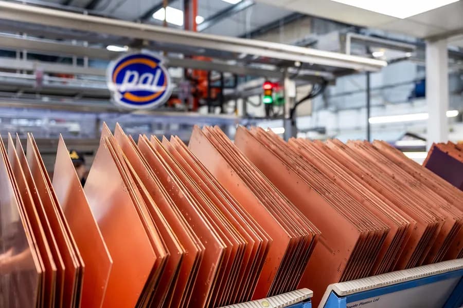
Close-up of a large rack of copper printed circuit board panels awaiting processing, under PAL branding.

Chinese New Year and PCB Supply Chains

Chinese New Year supply chain shutdowns can affect PCB material availability globally. Exception PCB manufactures in the UK year-round, but early planning on materials, lead times, and substitutions protects time-critical programmes from disruption.

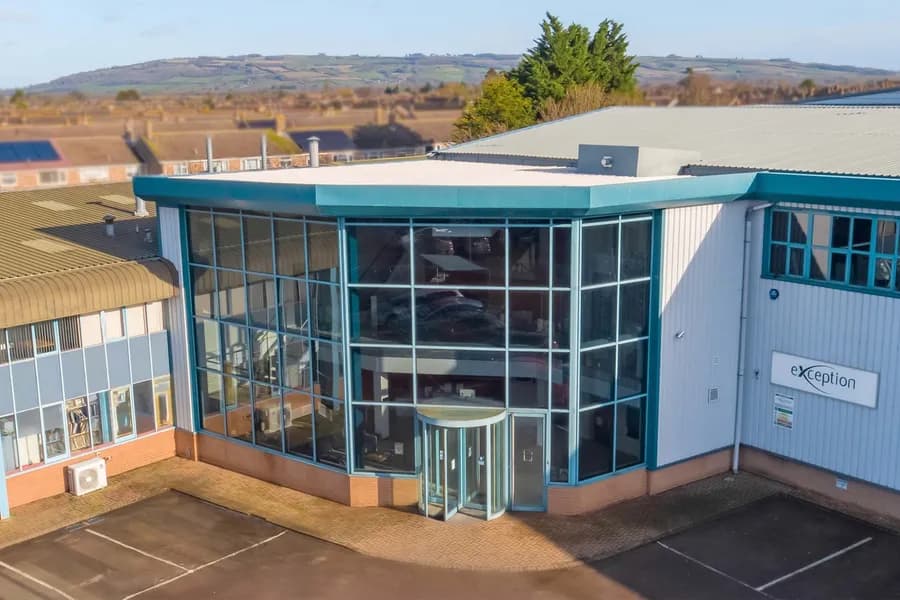
Exception PCB manufacturing facility in Tewkesbury, UK, supporting high-technology printed circuit board production.

Exception PCB Brought Back into British Ownership

Wright Industries has acquired Exception PCB, returning the Tewkesbury-based PCB manufacturer to UK ownership as part of the Connexion Technologies group, strengthening national manufacturing resilience.

RELATED PCB SERVICES

PCB manufacturing operator handling large printed circuit board panels during inspection at Exception PCB’s UK facility.

UK PCB Manufacturing

Exception PCB manufactures complex printed circuit boards from our 58,000 sq. ft. facility in Tewkesbury. Engineering-led process control, full traceability, and UK supply-chain resilience for regulated and performance-critical sectors

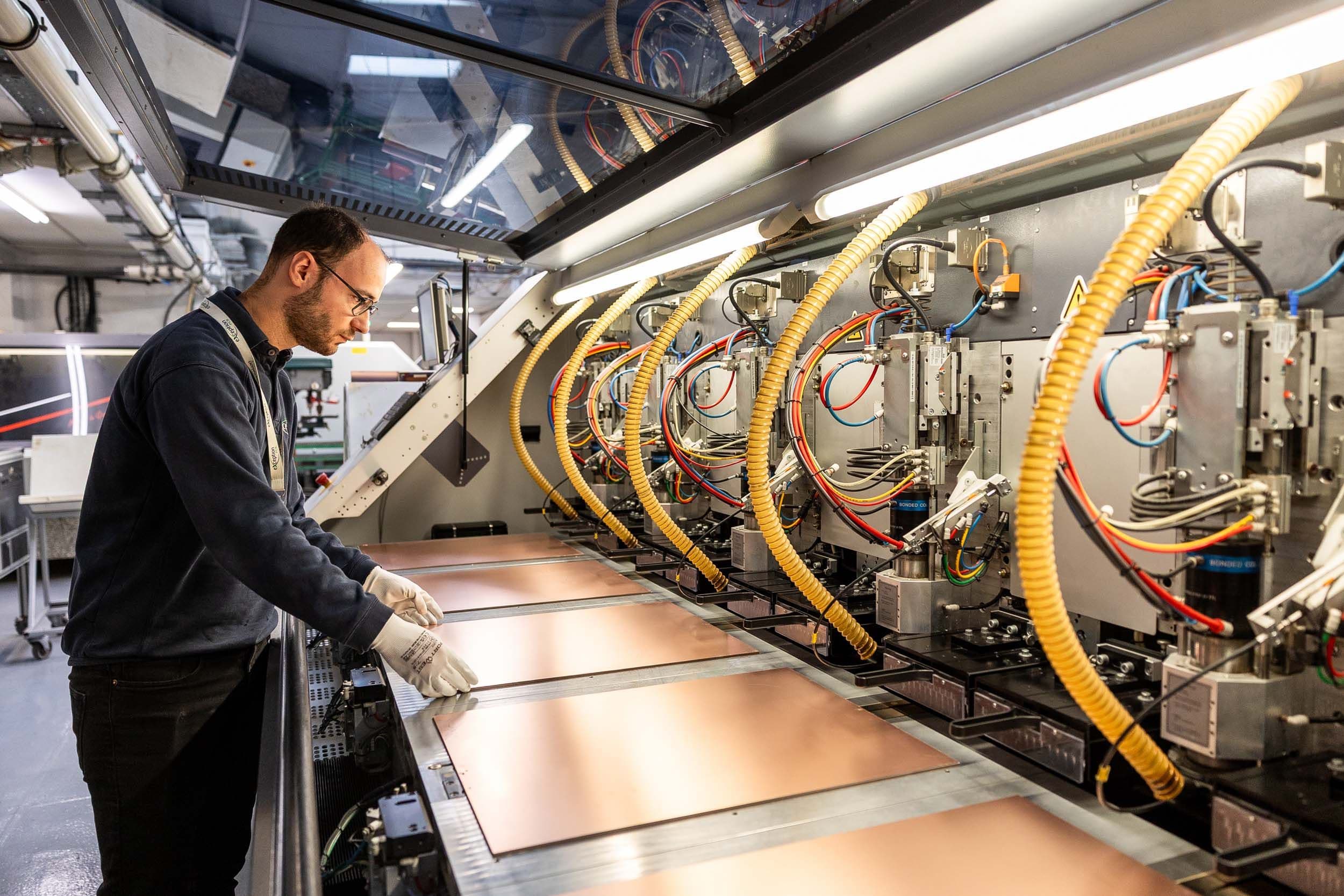
An Exception PCB technician loading copper production panels into a multi-station Schmoll CNC drilling machine.

Quick-Turn PCBs

Exception PCB's quick-turn service delivers accelerated PCB manufacturing for time-critical prototype and production builds, with the same process control and quality discipline applied to every order.

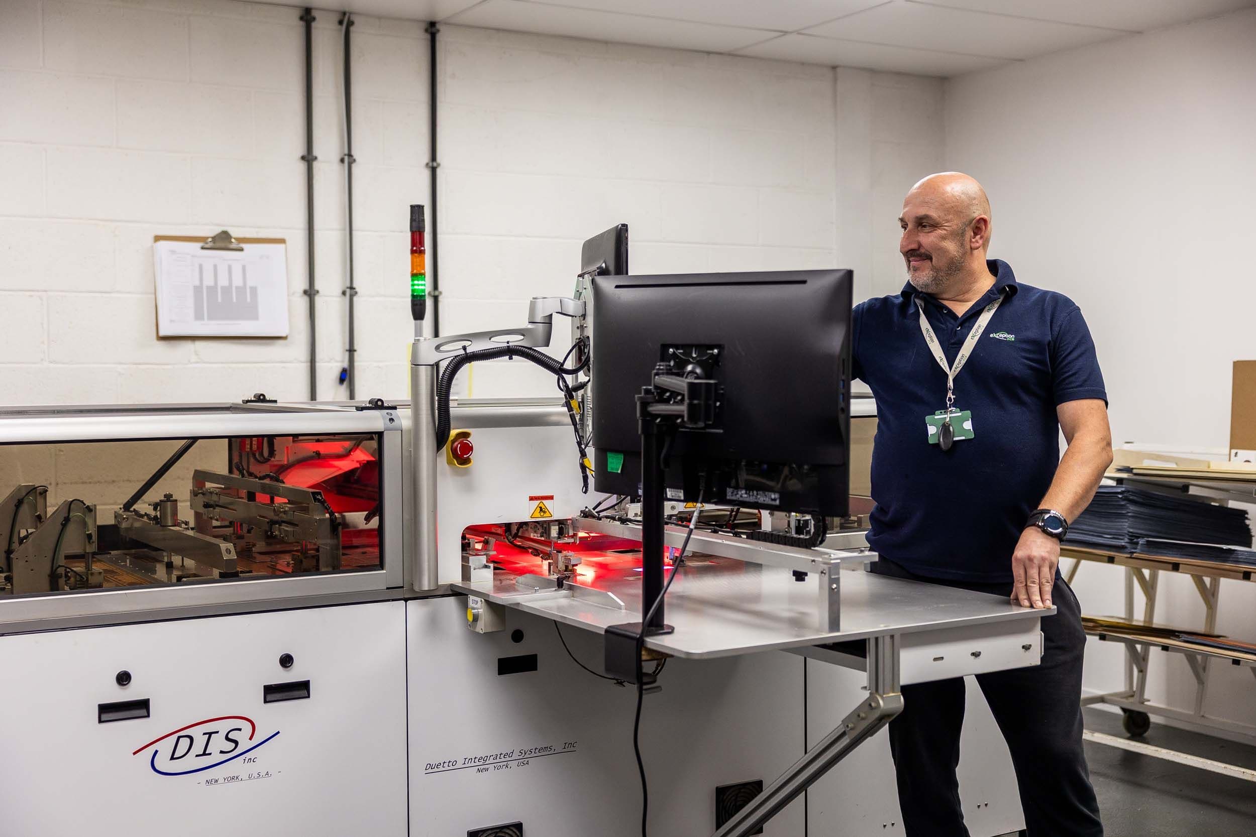
A smiling senior technician standing next to a Duetto Integrated Systems multilayer bonding machine at Exception PCB.

Research & Development

Exception PCB provides comprehensive engineering-led R&D support for new PCB materials and novel stack-ups. Our dedicated R&D team guides customers from initial requirements through to production-ready qualification and UL certification.

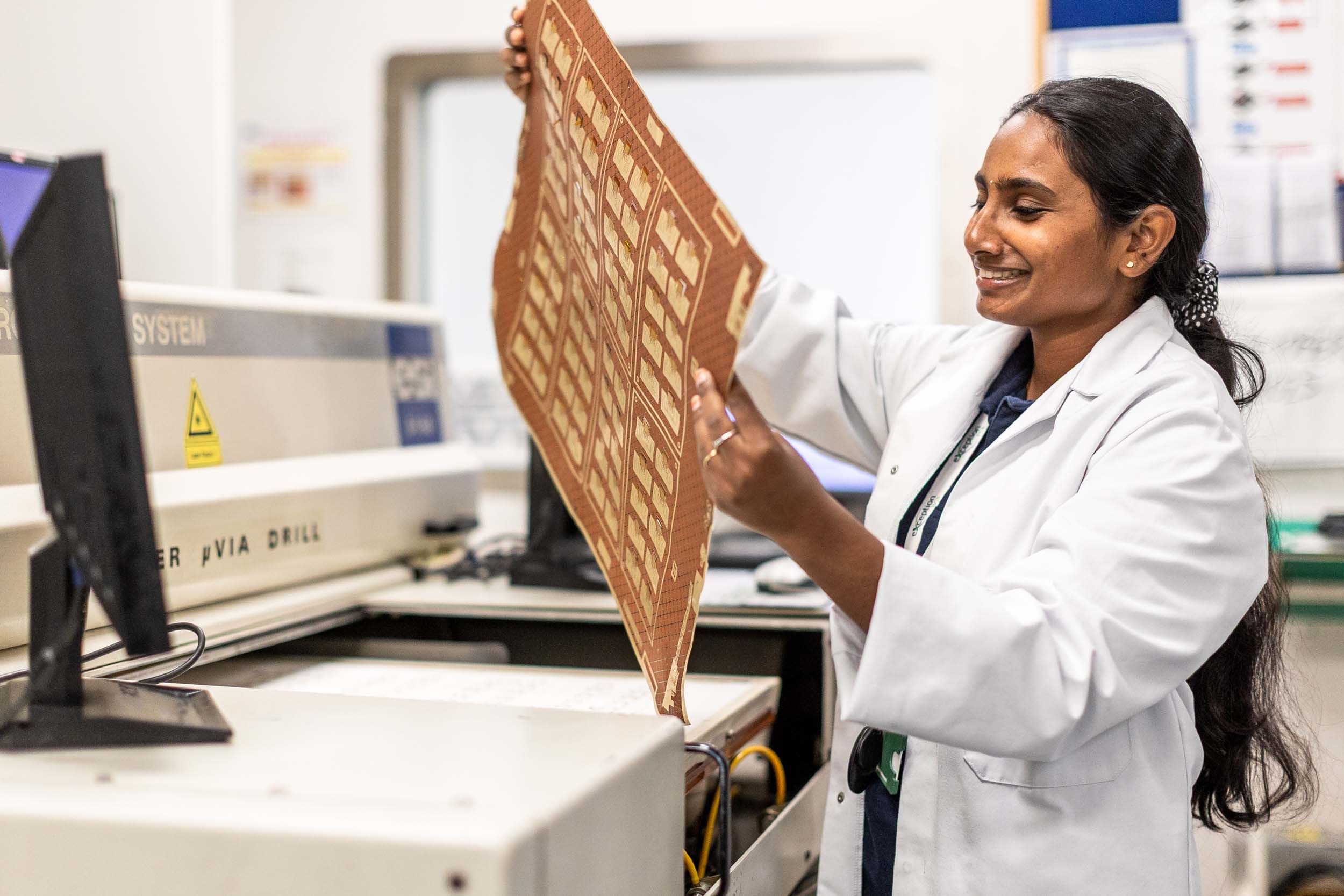
Side profile of a smiling Exception PCB engineer holding a flexible circuit sheet next to a micro via drill.

Design for Manufacture

Exception PCB provides engineering-led DFM review from an in-house team of ten engineers, identifying manufacturability risks and optimising designs before production begins. Available as an integrated or standalone service.