
PCB Technical Capabilities
A practical guide to our PCB manufacturing capabilities, tolerances, materials, and processes. Use it to qualify Exception PCB as a supplier, review design requirements, and prepare projects for manufacture.
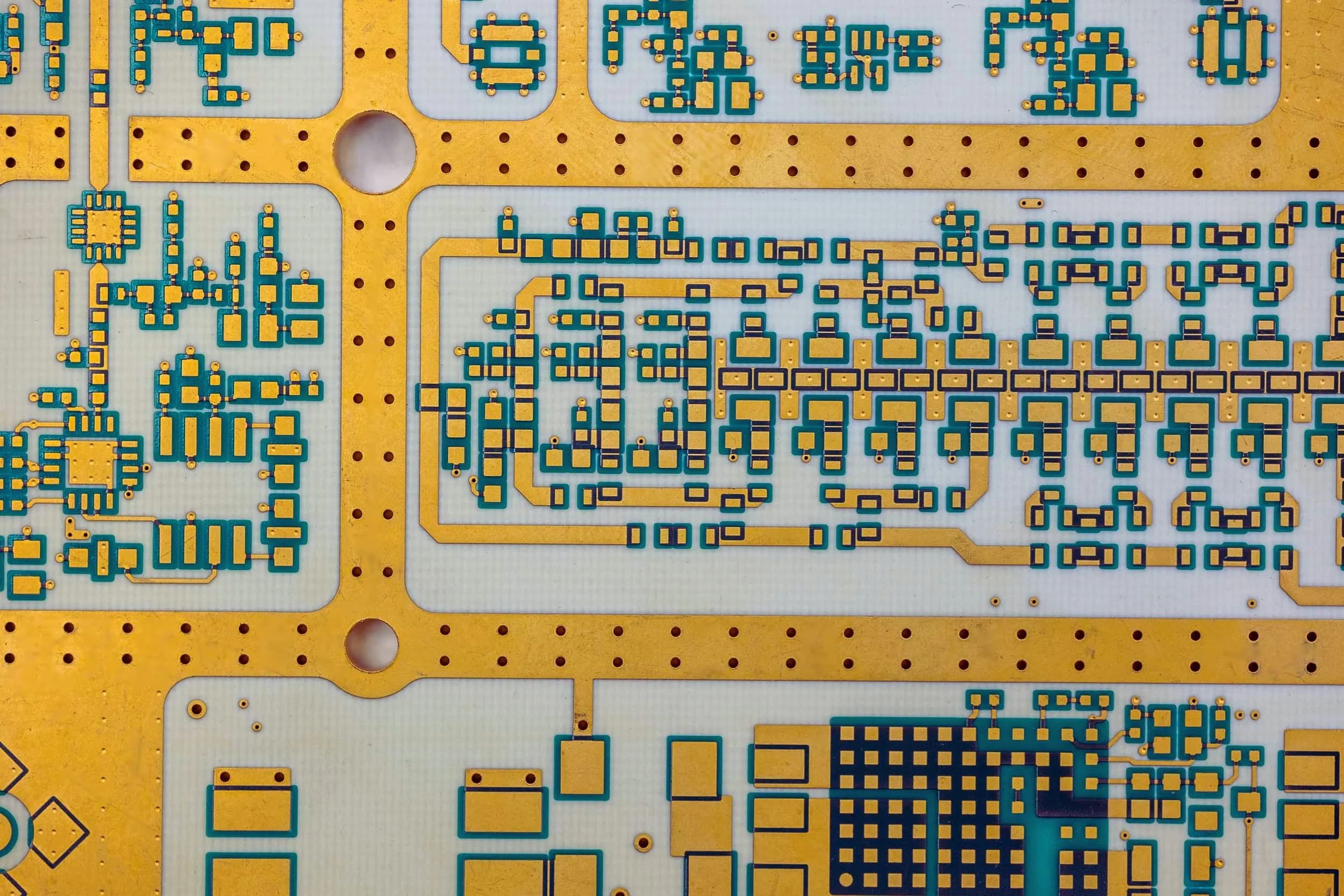
Engineering-led RF and microwave PCB manufacturing from our UK facility, supporting controlled impedance, low-loss performance, and consistent signal integrity in high-frequency applications.
RF PCB manufacture demands tighter control than conventional multilayer fabrication. At high frequencies, small variations in dielectric thickness, copper profile, surface finish, and layer registration directly influence signal performance. Exception PCB manufactures RF and microwave PCBs using controlled material systems, stable multilayer processing, and engineering-led stack-up design.
Our engineers work with OEMs developing RF architectures for communications, aerospace, defence, sensing, and high-speed digital systems. Material selection, via structures, copper foil choice, and surface finish are reviewed alongside frequency range and assembly requirements to ensure consistent performance in prototype and production.
Find answers on material options, controlled impedance tolerances, track widths, and frequency ranges.
The following capability ranges summarise the RF PCB manufacturing infrastructure available within Exception PCB’s production environment.
| CAPABILITY | ADVANCED CAPABILITY |
|---|---|
| Maximum layer count | Up to 24 layers |
| Controlled impedance | ± 10% standard / ± 5% advanced |
| Track / gap capability | Down to 75 µm |
| Laser microvia diameter | Down to 50 µm |
| Mechanical drill diameter | Down to 0.105 mm |
| RF-compatible materials | PTFE, Rogers, Isola, low-loss FR4, hybrid laminates |
| Sequential lamination | Multi-bond lamination supported |
| Via structures supported | Blind, buried, stacked and staggered |
| Via filling capability | Copper-filled and resin-filled vias |
| Surface finishes | ENIG, immersion silver, immersion tin, hard gold |
| Copper foil options | Standard, low-profile and VLP copper |
| Electrical testing | 100% electrical test |
These capabilities allow Exception PCB to manufacture RF multilayer structures that support impedance control, low insertion loss, and stable high-frequency performance.
Engineering review confirms that material selection, stack-up geometry, and process parameters remain aligned with RF design intent.
READY TO DISCUSS YOUR RF PCB REQUIREMENTS?
Our engineers can review your material selection, stack-up design, and impedance specification to confirm your RF PCB is manufacturable to specification.
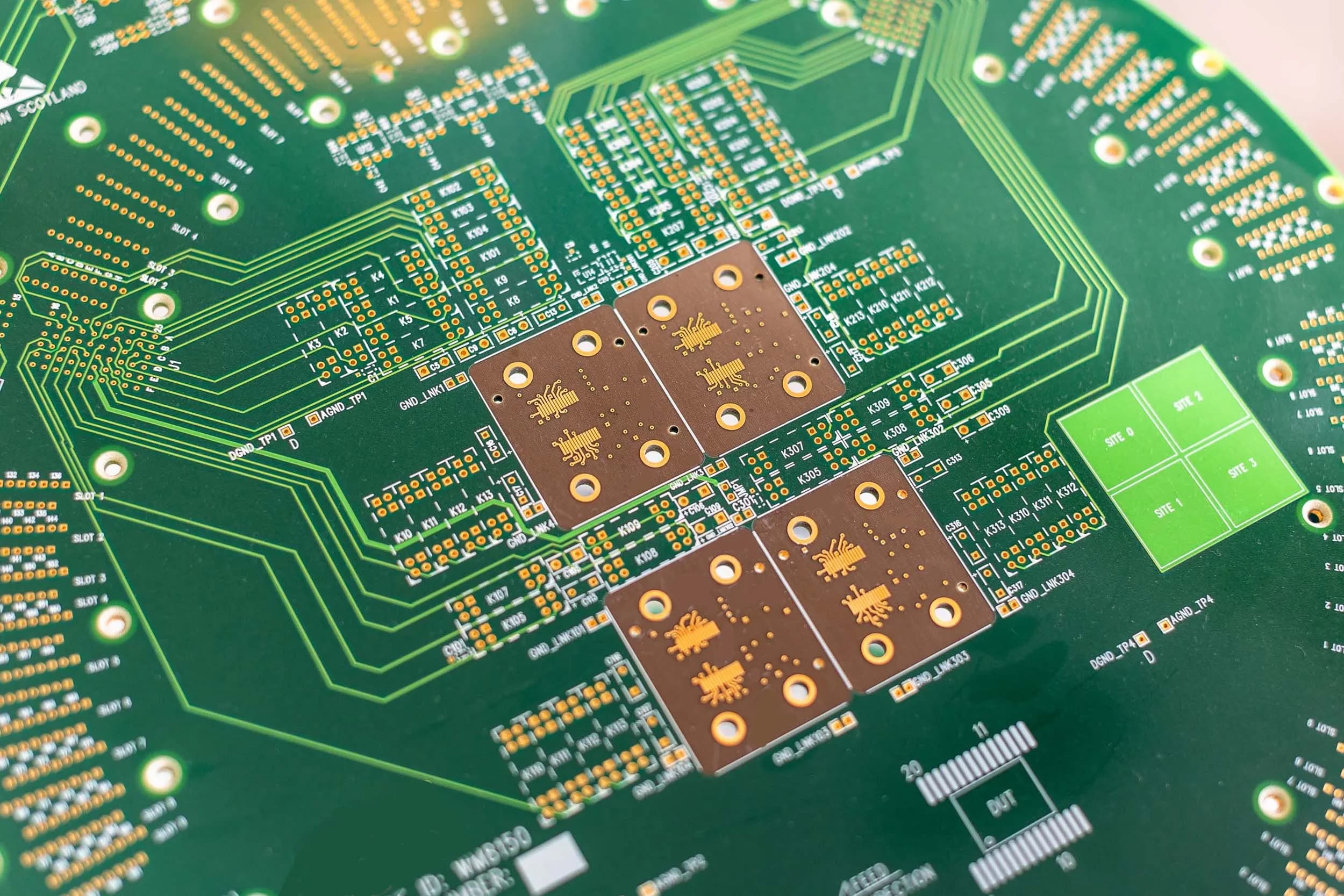
Material performance is central to RF PCB manufacture.
Dielectric stability, dissipation factor, and thermal behaviour influence insertion loss, impedance consistency, and signal propagation.
Exception PCB supports a broad range of RF-compatible materials including:
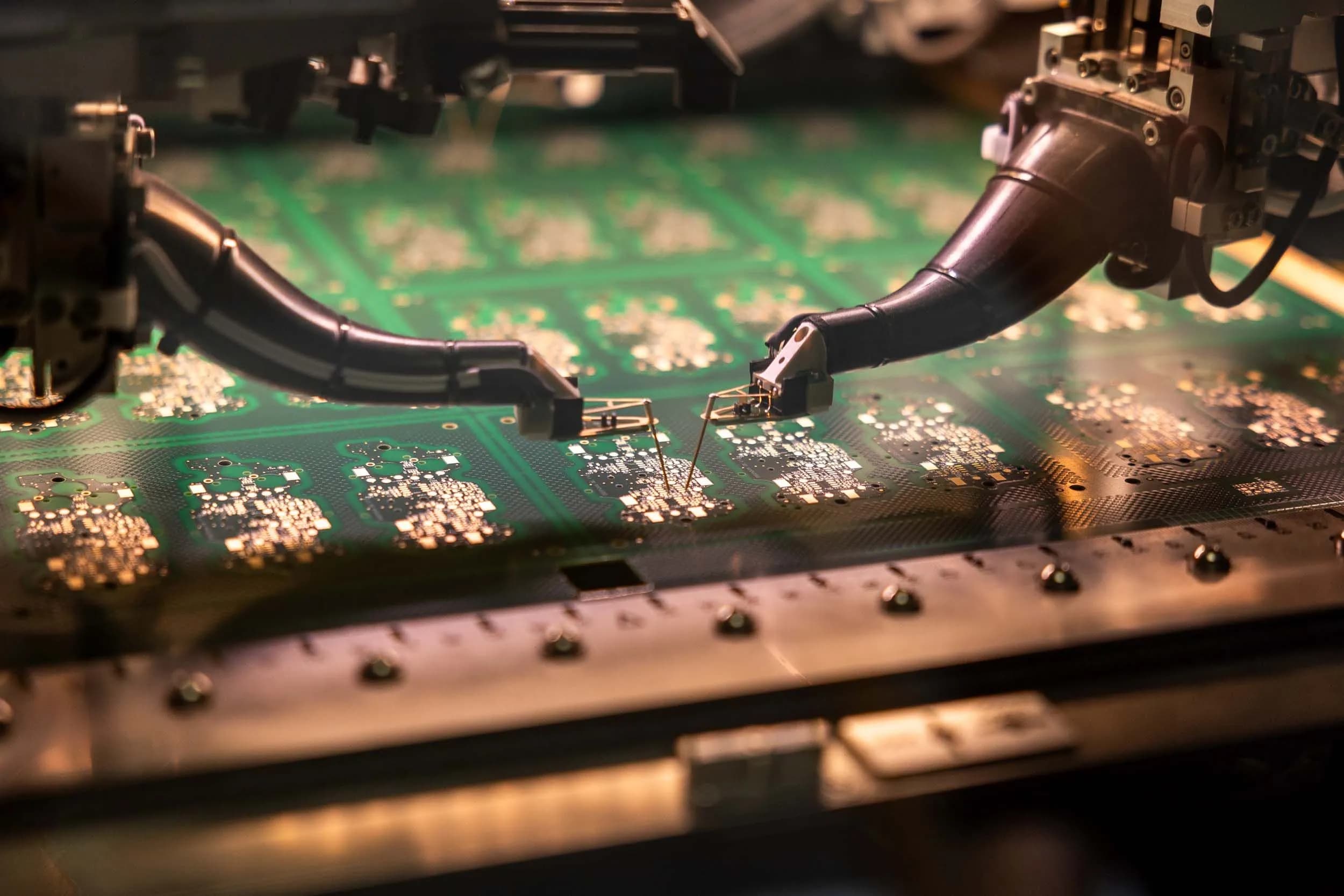
RF PCB performance depends on maintaining predictable impedance throughout the signal path.
Exception PCB integrates impedance control within stack-up definition and manufacturing planning.
Critical variables include:
Engineering review ensures impedance targets remain achievable within real manufacturing tolerances rather than theoretical assumptions.

At RF frequencies, conductor behaviour becomes increasingly sensitive to copper surface profile.
Copper roughness influences:
Exception PCB supports low-profile and very low-profile copper foils where high-frequency performance requires tighter conductor control.
Copper selection is considered alongside frequency range, insertion loss targets, and laminate compatibility.
Via behaviour can significantly affect RF signal integrity.
Transition inductance, via stubs, and grounding strategy influence electrical performance across high-frequency circuits.
Engineering review ensures via architecture supports the intended signal path and grounding structure.
EXCEPTION PCB SUPPORTS RF-SPECIFIC VIA STRATEGIES INCLUDING:
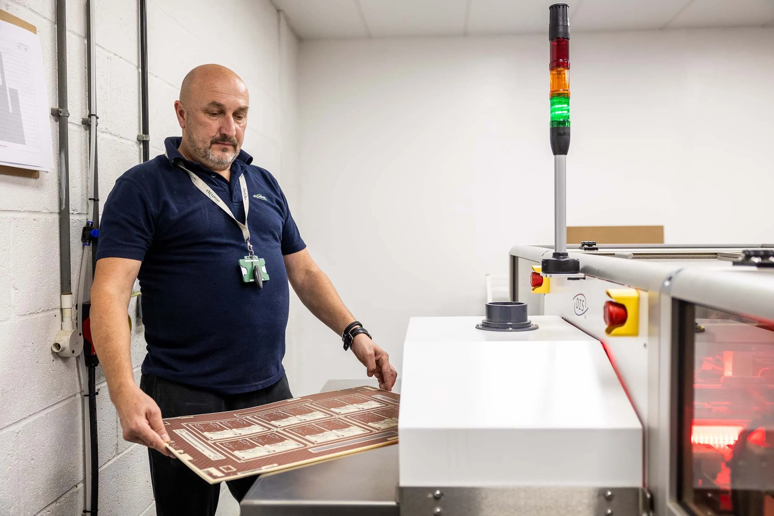
Many RF systems combine high-frequency routing with digital, power, or control circuitry.
Exception PCB manufactures hybrid stack-ups that integrate RF laminates alongside conventional multilayer materials.
These structures support:
Stack-up planning considers dielectric compatibility, expansion behaviour, and lamination stability.
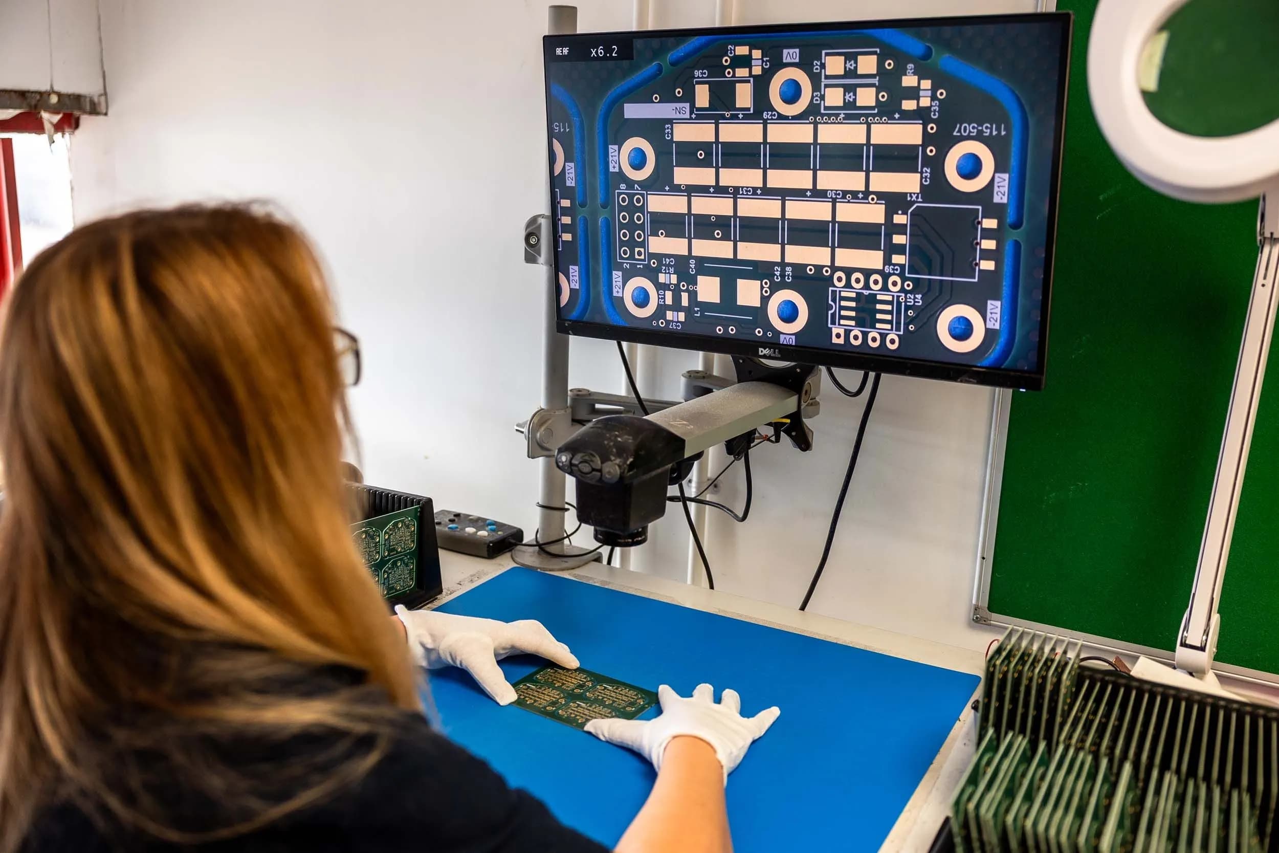
RF PCB manufacture requires controlled processing to maintain repeatable electrical performance.
Exception PCB integrates inspection and validation throughout manufacture.
INSPECTION INCLUDES:
These controls help ensure RF structures remain aligned with manufacturing intent.
RF PCBs are specified for systems where signal integrity, insertion loss, and phase consistency at high frequencies directly affect system performance. Manufacturing tolerances that are acceptable for standard digital designs can cause measurable degradation at microwave frequencies.

RADAR AND SENSING SYSTEMS
Phased array and pulse radar designs require consistent dielectric properties and repeatable impedance control across the full panel. Variation in copper roughness, laminate thickness, or etch accuracy directly translates to performance inconsistency across antenna elements.

DEFENCE RF ELECTRONICS
RF assemblies for airborne and defence applications combine demanding electrical specifications with environmental qualification requirements. Laminates must maintain stable electrical properties across wide temperature ranges, and manufacturing traceability is required throughout.

SATELLITE AND SPACE SYSTEMS
Satellite RF hardware operates across wide frequency ranges in environments where thermal cycling is extreme and repair is not an option. Low-loss PTFE-based laminates are commonly specified, and stack-up design must account for thermal expansion compatibility across hybrid constructions.

AUTOMOTIVE RADAR AND ADAS
Advanced driver assistance systems use millimetre-wave radar operating above 76 GHz, where small deviations in conductor geometry affect beam performance. Consistent etch accuracy and controlled dielectric thickness are required across production volumes to maintain antenna pattern repeatability.
RF PCB performance begins during stack-up planning.
Exception PCB engineers work closely with customers to ensure material systems, via structures, and impedance targets remain aligned with manufacturable process capability.
Early engagement helps reduce development risk and supports reliable transition from prototype to production.
EXCEPTION PCB ENGINEERS REGULARLY REVIEW:
TALK TO OUR ENGINEERS
Whether you are developing microwave circuitry, RF multilayer systems, or mixed-technology architectures, Exception PCB can support the right manufacturing approach.
Below we have answered the questions our engineers are asked most often. If yours isn't covered, get in touch with the team directly.
RF PCBs typically use low-loss materials designed for stable dielectric performance at high frequencies.
COMMON OPTIONS INCLUDE:
Material selection depends on frequency range, insertion loss requirements, thermal conditions, and multilayer architecture.
Controlled impedance ensures signal energy propagates predictably through the PCB structure.
IMPEDANCE VARIATION CAN CREATE:
Manufacturing control is essential to maintaining impedance targets.
At higher frequencies, current flows near the conductor surface.
Rough copper increases effective conductor path length and contributes to insertion loss.
Low-profile copper foils are often selected where signal loss must be minimised.
Yes. RF PCB designs frequently incorporate HDI features such as microvias and sequential lamination.
HDI INTEGRATION SUPPORTS:
Engineering review ensures HDI structures remain compatible with RF material systems.
Validation includes both dimensional and structural inspection.
TYPICAL CONTROLS INCLUDE:
These steps confirm that RF performance-critical structures remain within manufacturing tolerance.
Explore guides and references covering PCB construction types, laminate selection, and the full range of capabilities available at Exception PCB.
Explore related technologies that help control signal integrity, material performance, via structures and manufacturability in complex RF PCB designs.
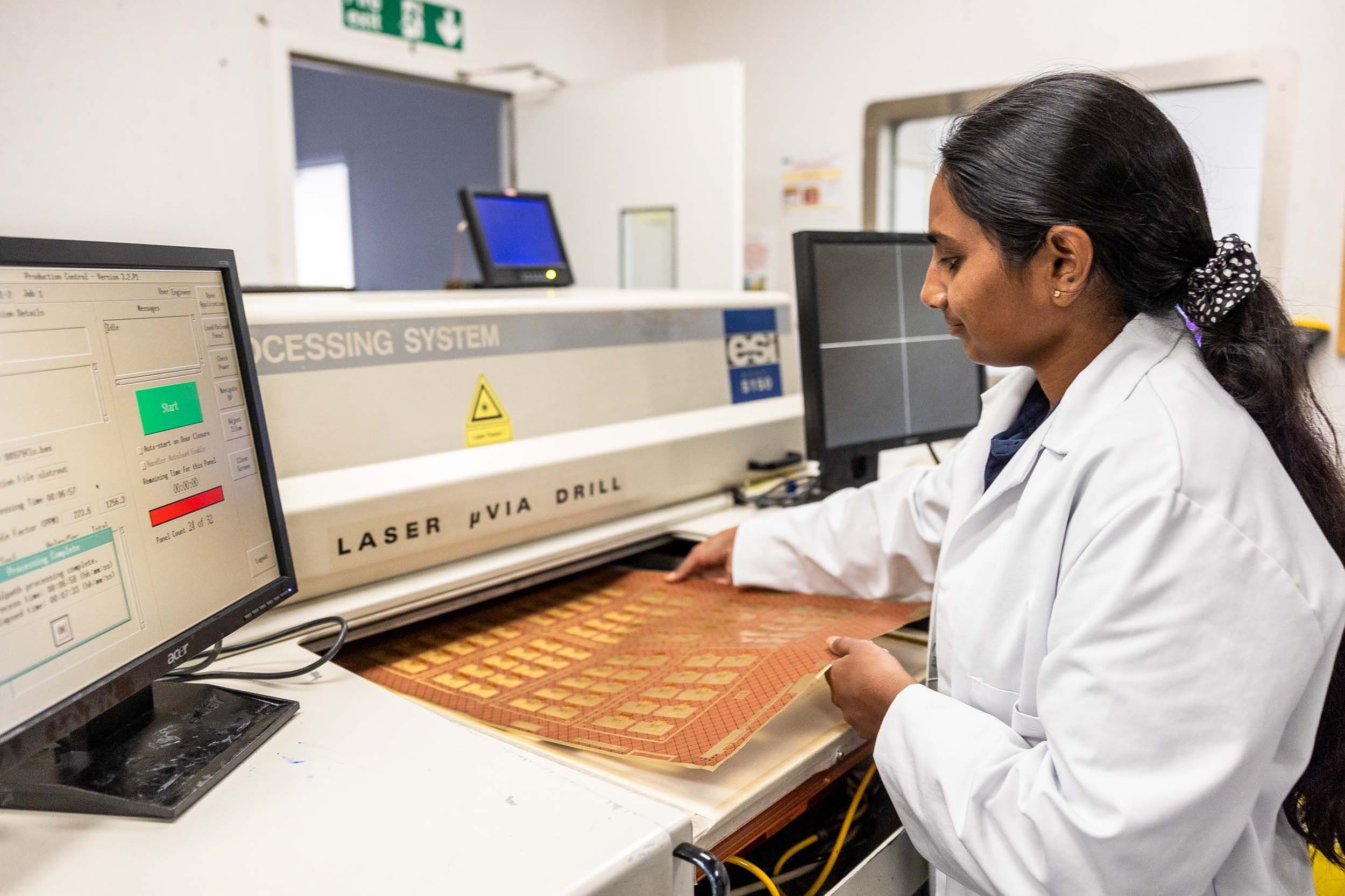
Support for specialist and hybrid PCB materials selected to meet thermal, electrical, and environmental performance requirements in applications where standard FR4 or conventional laminate systems cannot deliver the required performance.
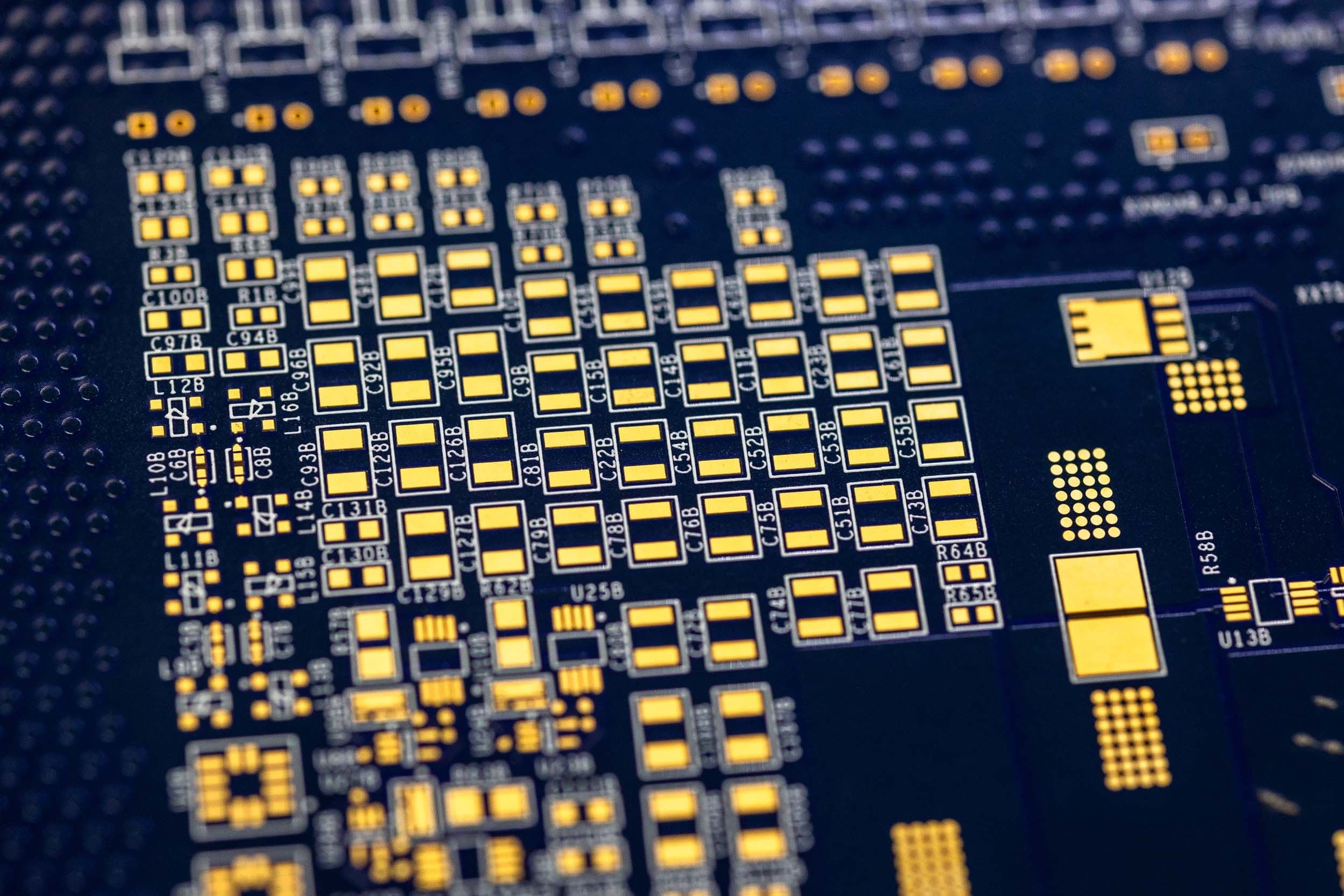
High-density interconnect PCBs for fine features, microvias, and complex multilayer designs, manufactured using production-ready processes with full engineering oversight to ensure reliable and repeatable fabrication of the most demanding constructions.
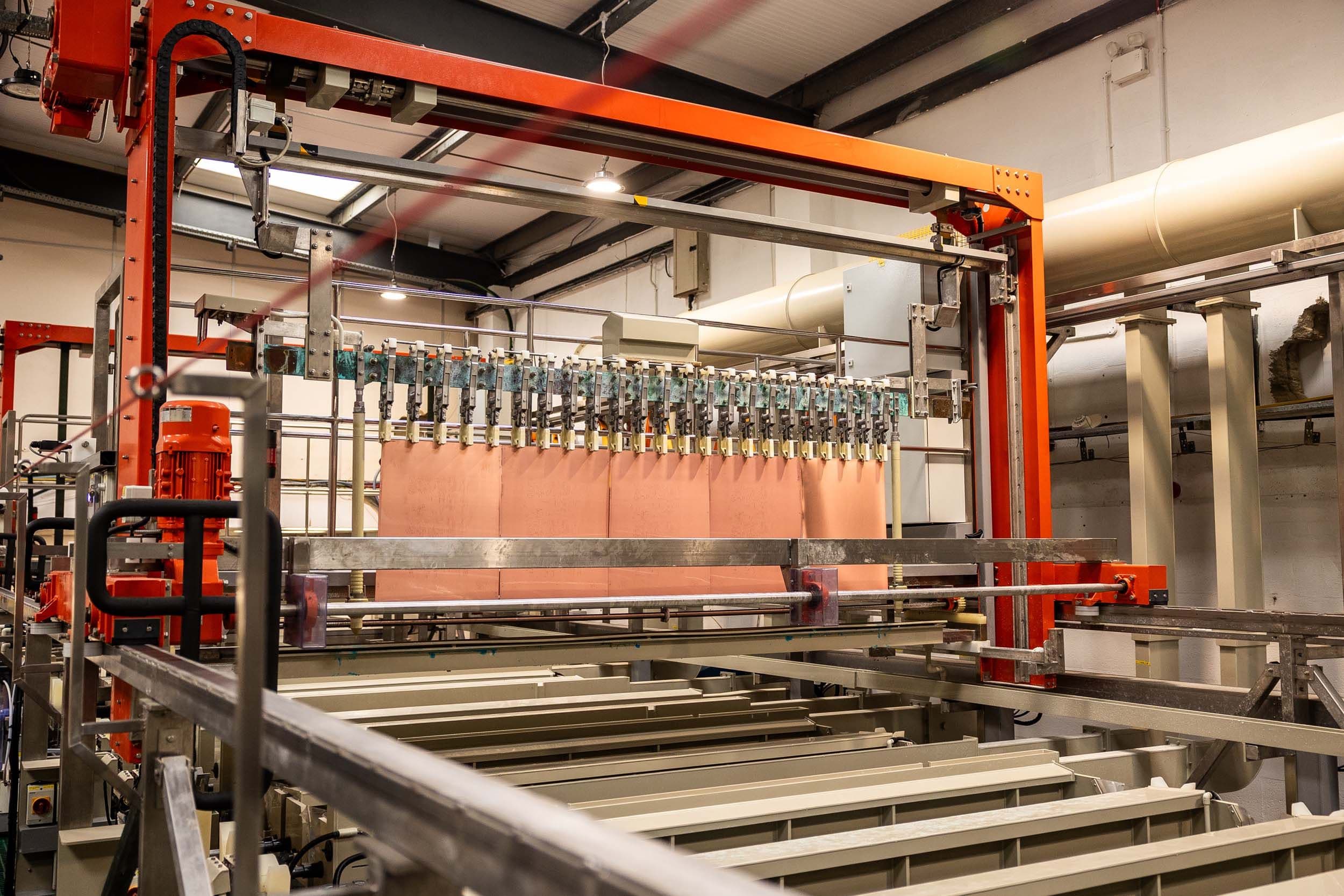
Copper via filling for blind, buried, and through-hole vias, supporting HDI constructions, via-in-pad designs, and thermally demanding multilayer PCBs where electrical continuity, thermal performance, and consistent fill quality are required.
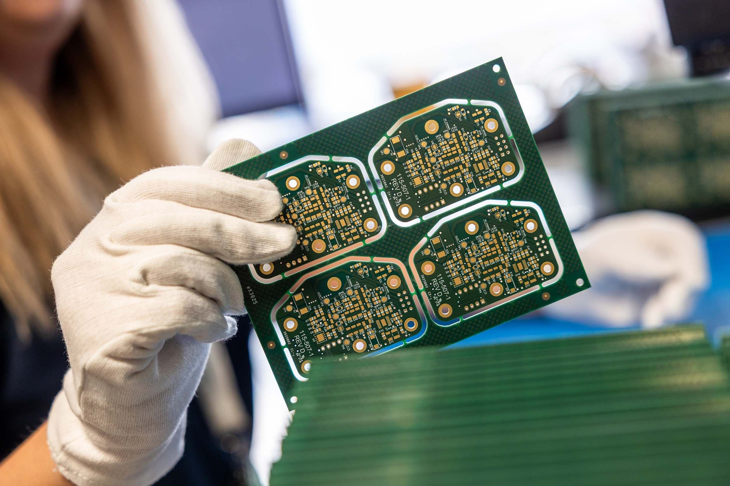
Resin via fill for blind, buried, and through-hole vias, providing consistent surface planarity to support via-in-pad designs, fine-pitch assembly, and sequential lamination builds where assembly quality and via integrity matter.
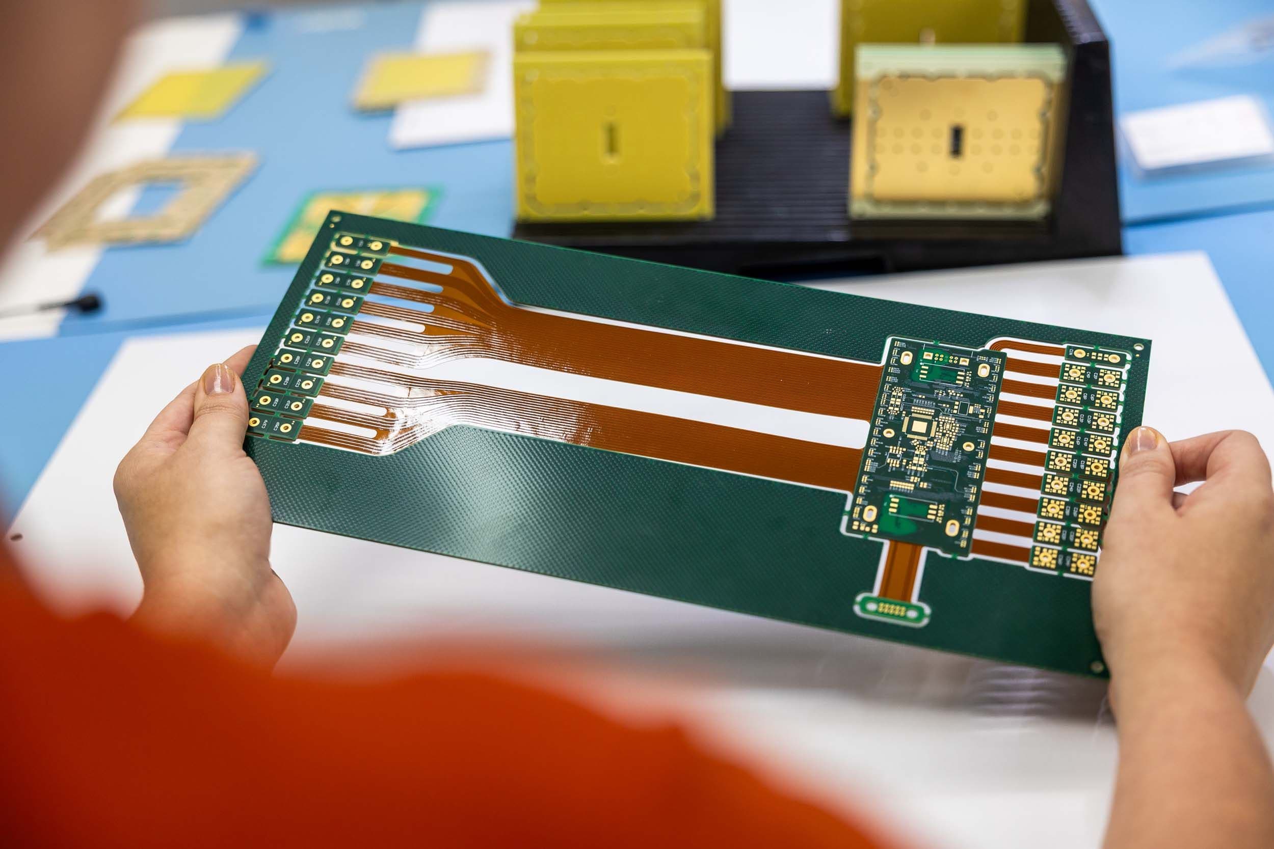
Complex flex and rigid-flex PCB constructions for space-constrained and dynamic applications, built with reliability and repeatability in mind to support confident integration where weight, form factor, or movement are critical.