
PCB Technical Capabilities
A practical guide to our PCB manufacturing capabilities, tolerances, materials, and processes. Use it to qualify Exception PCB as a supplier, review design requirements, and prepare projects for manufacture.
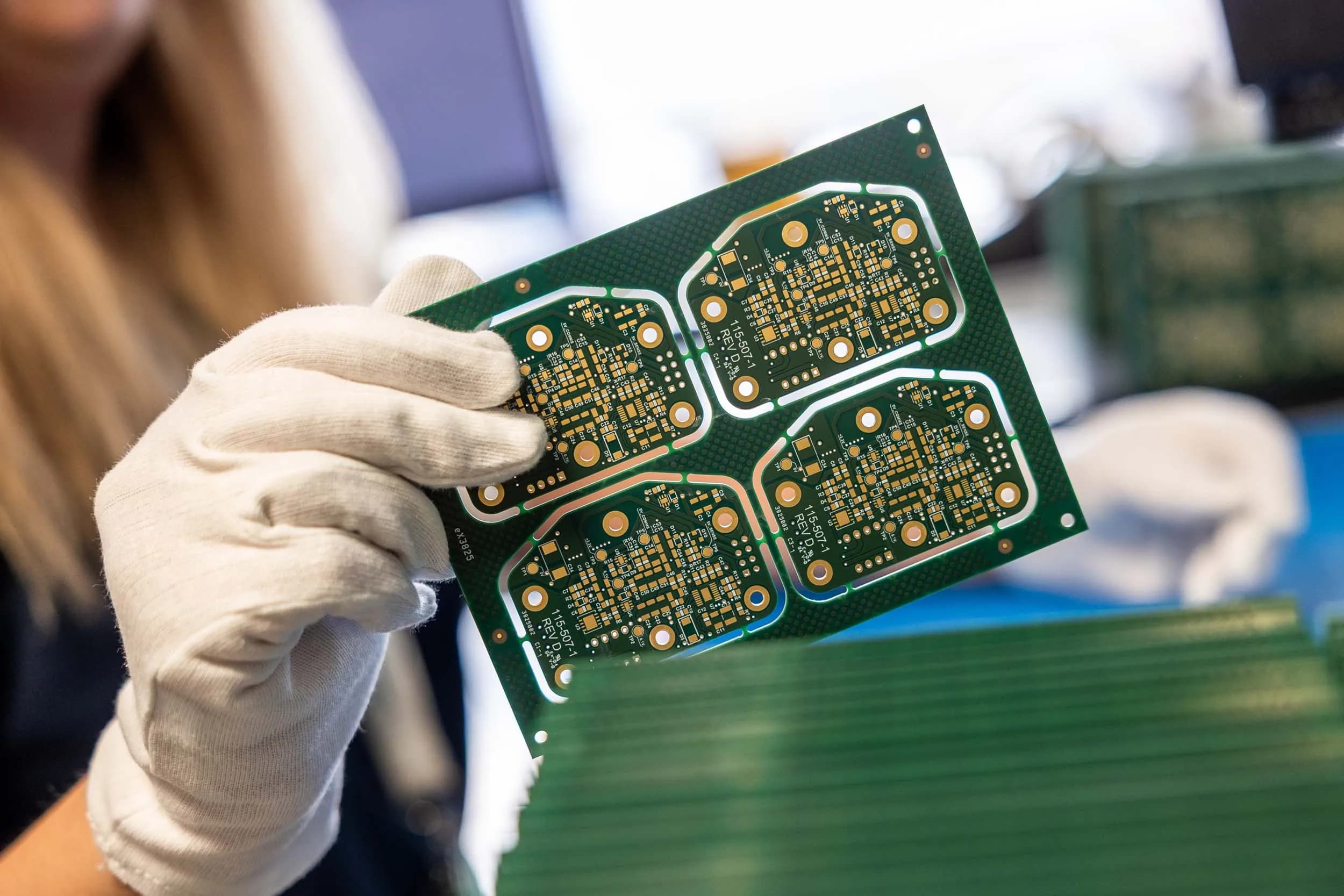
Engineering-led resin via fill manufacturing from our UK facility, supporting surface planarity, stacked via architectures, and dense multilayer PCB designs.
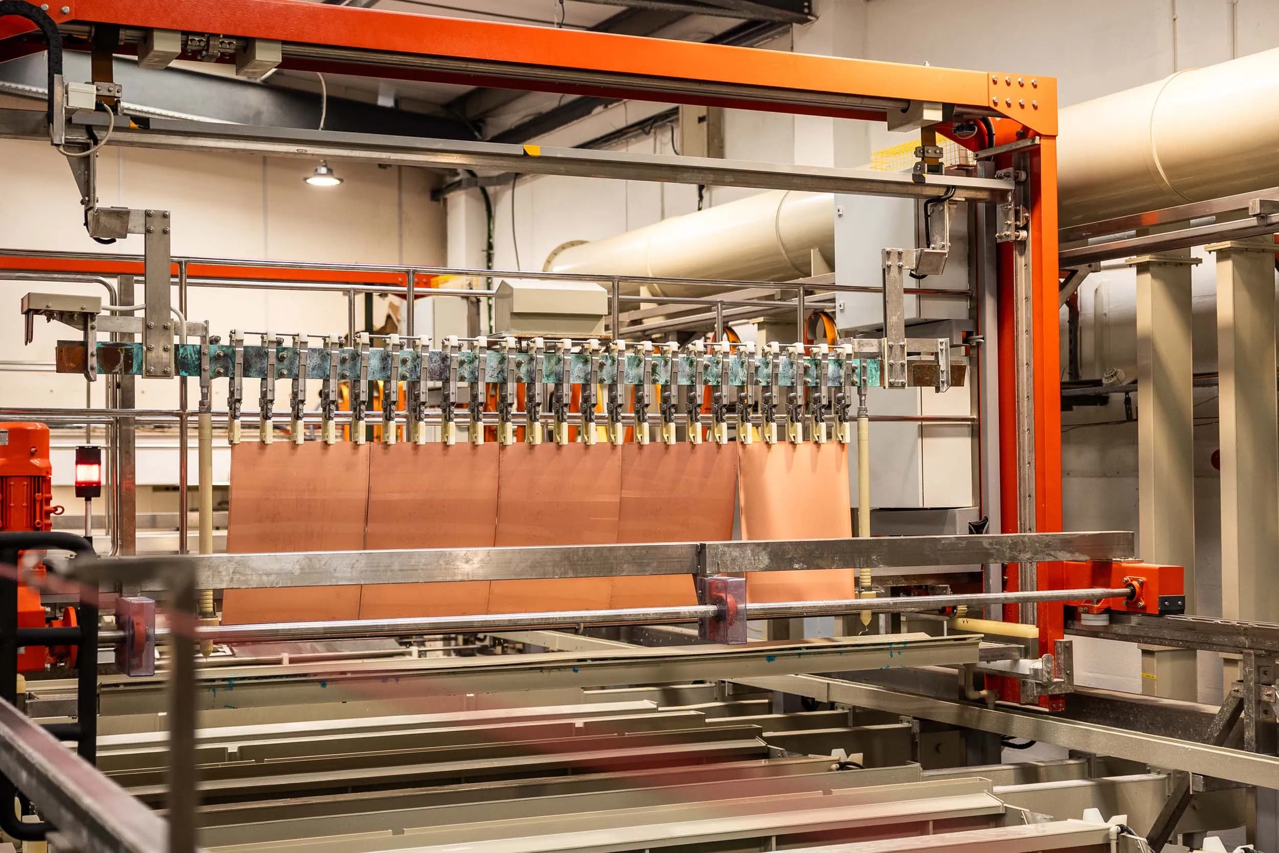
Copper via fill uses controlled electrolytic plating to deposit copper uniformly within blind, buried, and through-hole via structures, supporting HDI constructions, via-in-pad configurations, and thermally demanding multilayer designs. Exception PCB manufactures copper-filled via structures using tightly controlled plating chemistry, current distribution, and process monitoring to ensure complete fill, consistent conductivity, and structural integrity.
Our engineers review via geometry, stack-up structure, and plating parameters before production begins, ensuring each specification is achievable within stable manufacturing limits. For designs incorporating stacked microvias, high-power components, or fine-pitch assembly requirements, early engineering engagement helps align the via strategy with both design intent and long-term reliability.
Find answers on via geometries supported, planarisation tolerances, resin fill consistency, and stack-up compatibility.
Our resin via fill process is engineered for repeatability, dimensional control, and compatibility with complex multilayer builds.
We manufacture resin-filled vias across a broad range of board constructions, supported by advanced drilling, plating, and planarisation capability.
| CAPABILITY | TYPICAL CAPABILITY |
|---|---|
| Via structures supported | Blind, buried and through-hole vias |
| Minimum laser microvia diameter | 75 µm |
| Minimum mechanical drill diameter | 0.105 mm |
| Typical resin-filled via diameter range | 0.20 mm – 0.60 mm |
| Maximum via aspect ratio | Up to 10:1 |
| Microvia aspect ratio | Up to 1:1 |
| Via filling methods | Resin-filled, resin-filled and capped Supported for HDI and fine-pitch assembly |
| Via-in-pad support | Supported for HDI and fine-pitch assembly |
| Compatible PCB constructions | Multilayer, HDI, RF, flex and rigid-flex |
| Planarisation process | Surface planarisation for pad-flatness and lamination readiness |
| Inspection and validation | Microsection analysis and cross-section verification |
| Reliability validation | Process validation for thermal cycling performance |
| Electrical testing | 100% electrical test |
These capabilities allow Exception PCB to manufacture resin-filled via structures that support planar surfaces, stacked via architectures, and high-density multilayer PCB designs while maintaining consistent assembly performance and mechanical stability.
Engineering review is used to confirm that via geometry, stack-up architecture, resin selection, and planarisation requirements remain within stable manufacturing limits for the intended application.
READY TO DISCUSS YOUR VIA FILL REQUIREMENTS?
Our engineers can review your via geometry, planarisation requirements, and stack-up architecture to confirm your design meets manufacturing limits.
Resin via fill performance depends on far more than simply filling the hole.
At Exception PCB, the process sits within a controlled manufacturing route designed to ensure fill consistency, adhesion integrity, and surface planarity.
CONTROLLED MANUFACTURING FLOW
1. Precision mechanical or laser drilling
2. Hole preparation and desmear
3. Resin filling under controlled deposition parameters
4. Thermal cure cycle
5. Surface planarisation
6. Copper plating integration
7. Cross-section validation and inspection
This approach minimises void formation, improves via integrity, and supports downstream assembly performance.
Resin-filled vias are often integrated into multilayer PCB architectures where routing density and layer transitions demand tighter interconnect control.
Surface planarity is a direct outcome of the fill and planarisation process: the resin creates a sealed, flat surface across the via opening, eliminating the depression that an unfilled via leaves and providing a stable base for pad-level copper cap plating.
EXCEPTION PCB SUPPORTS RESIN VIA FILL WITHIN:
Because resin via fill sits within the wider multilayer process, via performance is evaluated alongside lamination stability, plating behaviour, and material compatibility.
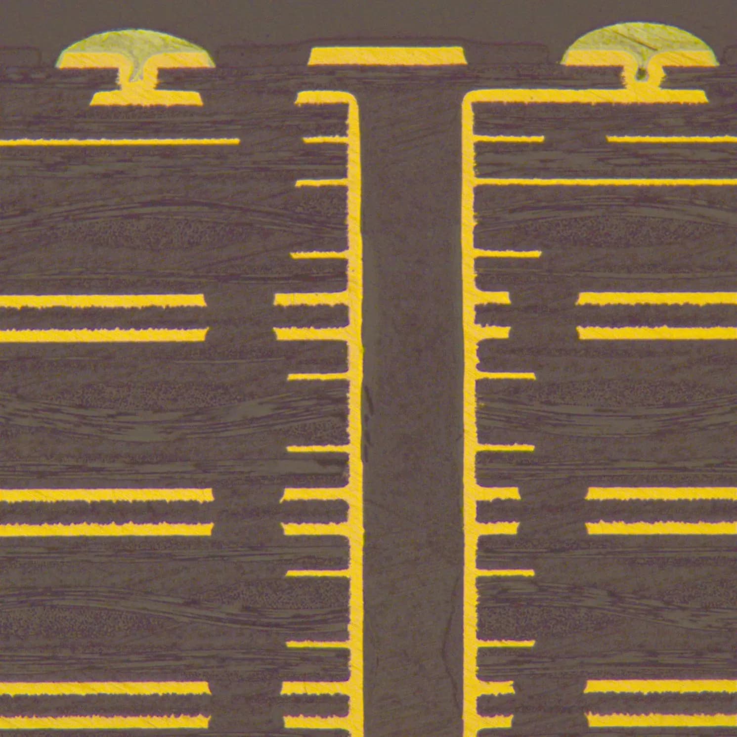
Cross-section of a resin-filled buried via with copper cap plating, producing a void-free, pad-level surface finish for reliable fine-pitch BGA and QFN component placement.
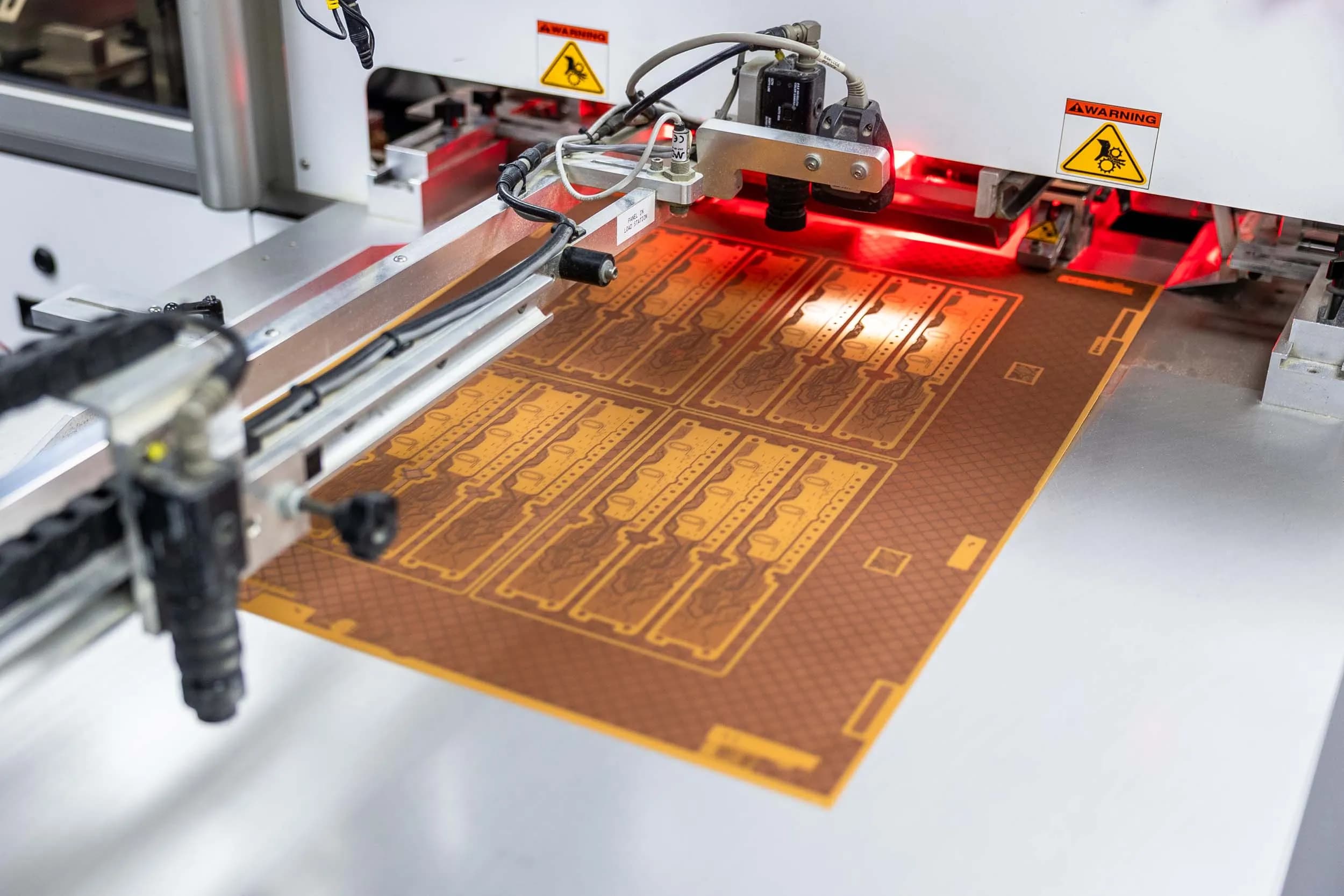
Resin-filled vias are often integrated into multilayer PCB architectures where routing density and layer transitions demand tighter interconnect control.
EXCEPTION PCB SUPPORTS RESIN VIA FILL WITHIN:
Because resin via fill sits within the wider multilayer process, via performance is evaluated alongside lamination stability, plating behaviour, and material compatibility.
Every resin via fill build follows a defined manufacturing route, with verification integrated at each stage from drill preparation through to surface planarisation and final inspection.
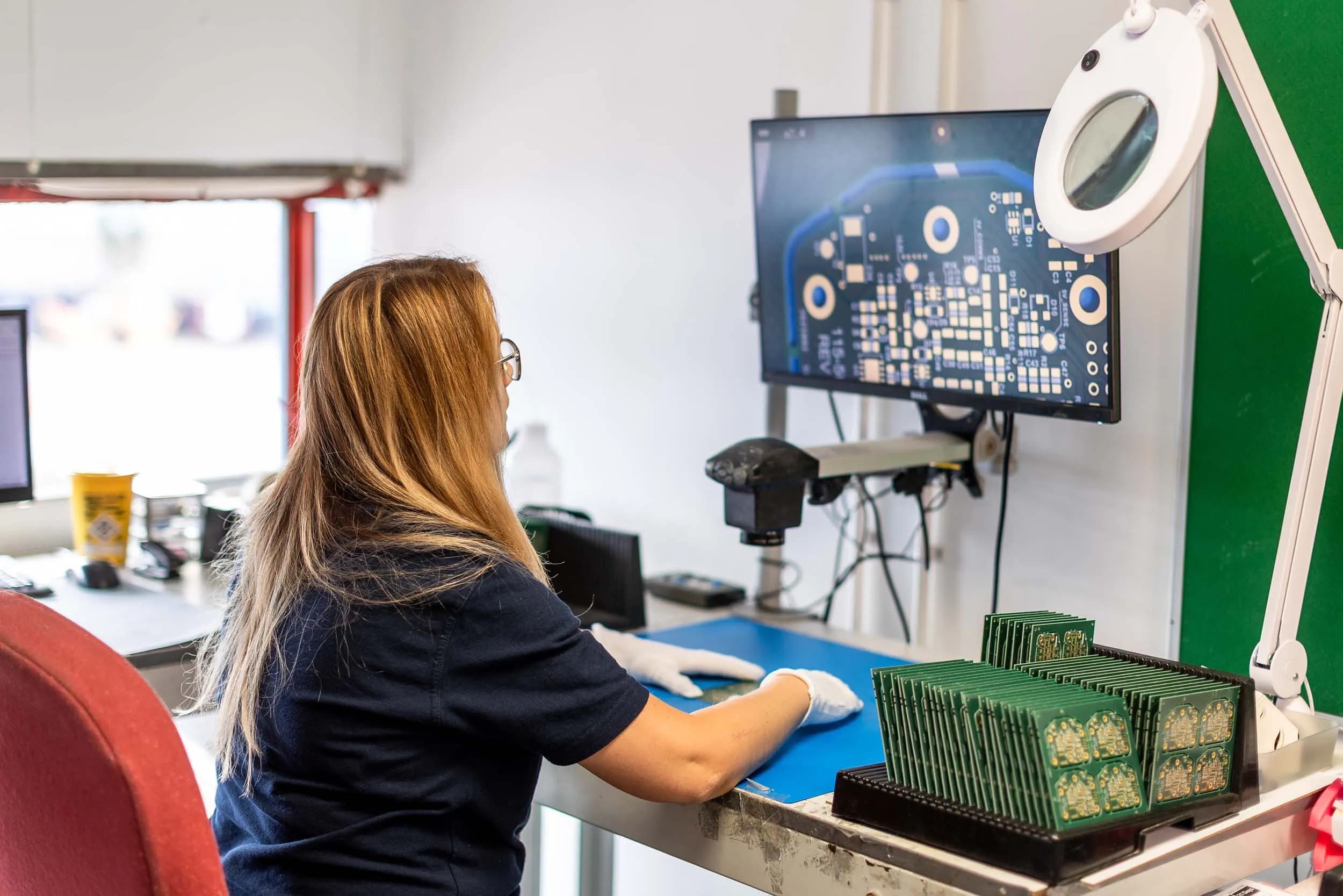
We support via fill quality through documented procedures, controlled process routes, and full traceability across every build.
OUR SYSTEMS SUPPORT:
Quality systems are aligned to AS9100 and ISO 9001, supporting customers in regulated sectors where documented manufacturing control is a programme requirement.
Resin via fill is specified where the surface condition of the PCB must meet the requirements of fine-pitch assembly processes, or where via integrity under thermal stress is a design requirement.
AEROSPACE AVIONICS
Avionics assemblies subject PCBs to repeated thermal cycling, and unfilled or poorly capped vias can allow moisture ingress or propagate cracks under mechanical stress. Resin fill with copper cap provides a sealed, stable interconnect that maintains integrity throughout the service life of the assembly.
MEDICAL INSTRUMENTATION
Miniaturised medical PCBs often carry BGAs and fine-pitch devices in areas of high routing density. Resin-filled and capped vias allow via-in-pad placement without the risk of solder wicking into open barrel vias, improving assembly consistency and long-term joint reliability.
SEQUENTIAL LAMINATION DESIGNS
Sequential lamination requires each lamination cycle to be built on a flat, stable surface. Resin-filled vias in earlier layers prevent resin bleed into open barrels during subsequent pressing cycles, maintaining dimensional stability and stack-up integrity across the build sequence.
RF AND MICROWAVE ASSEMBLIES
Surface planarity directly affects solder paste volume consistency during SMT assembly of RF components. Resin-filled and capped vias eliminate the surface depression that an open via leaves, ensuring consistent paste deposition under fine-pitch RF components where joint geometry affects electrical performance.
Resin via fill is often specified within HDI and fine-pitch assembly designs where surface planarity and via integrity are critical to manufacturing success.
Early engagement with the manufacturing team helps ensure fill specifications are compatible with the stack-up, lamination sequence, and surface finish requirements.
EXCEPTION PCB ENGINEERS SUPPORT DESIGN TEAMS BY REVIEWING:
TALK TO OUR ENGINEERS
If you are specifying filled vias for HDI or reliability-critical applications, our engineers can help define the right manufacturing approach.
Below we have answered the questions our engineers are asked most often. If yours isn't covered, get in touch with the team directly.
Resin-filled vias are primarily used to create a planar, sealed surface suitable for assembly and multilayer integration. Copper-filled vias are selected where electrical conductivity and thermal transfer through the via are critical.
Resin fill is commonly specified for:
Copper fill is typically used where higher thermal or electrical performance is required.
Via-in-pad layouts place vias directly beneath component pads. Open vias can draw solder away during reflow, affecting joint reliability.
Resin-filled vias create a sealed, flat surface that supports:
Yes. When properly manufactured, resin-filled vias provide strong mechanical stability during thermal cycling.
Reliability depends on:
Process validation helps ensure filled vias remain structurally stable over repeated thermal exposure.
Yes. Resin via fill is commonly integrated into HDI structures where dense routing and stacked vias require planar surfaces.
Exception PCB supports resin via fill within:
Filled vias are verified using inspection techniques that confirm fill quality and structural integrity.
Typical validation includes:
These processes ensure the filled via performs consistently within the finished PCB structure.
Explore guides and references covering PCB construction types, via structures, and the full range of capabilities available at Exception PCB.
Explore related technologies that support resin-filled via structures, surface planarity, assembly readiness and controlled multilayer PCB manufacture.
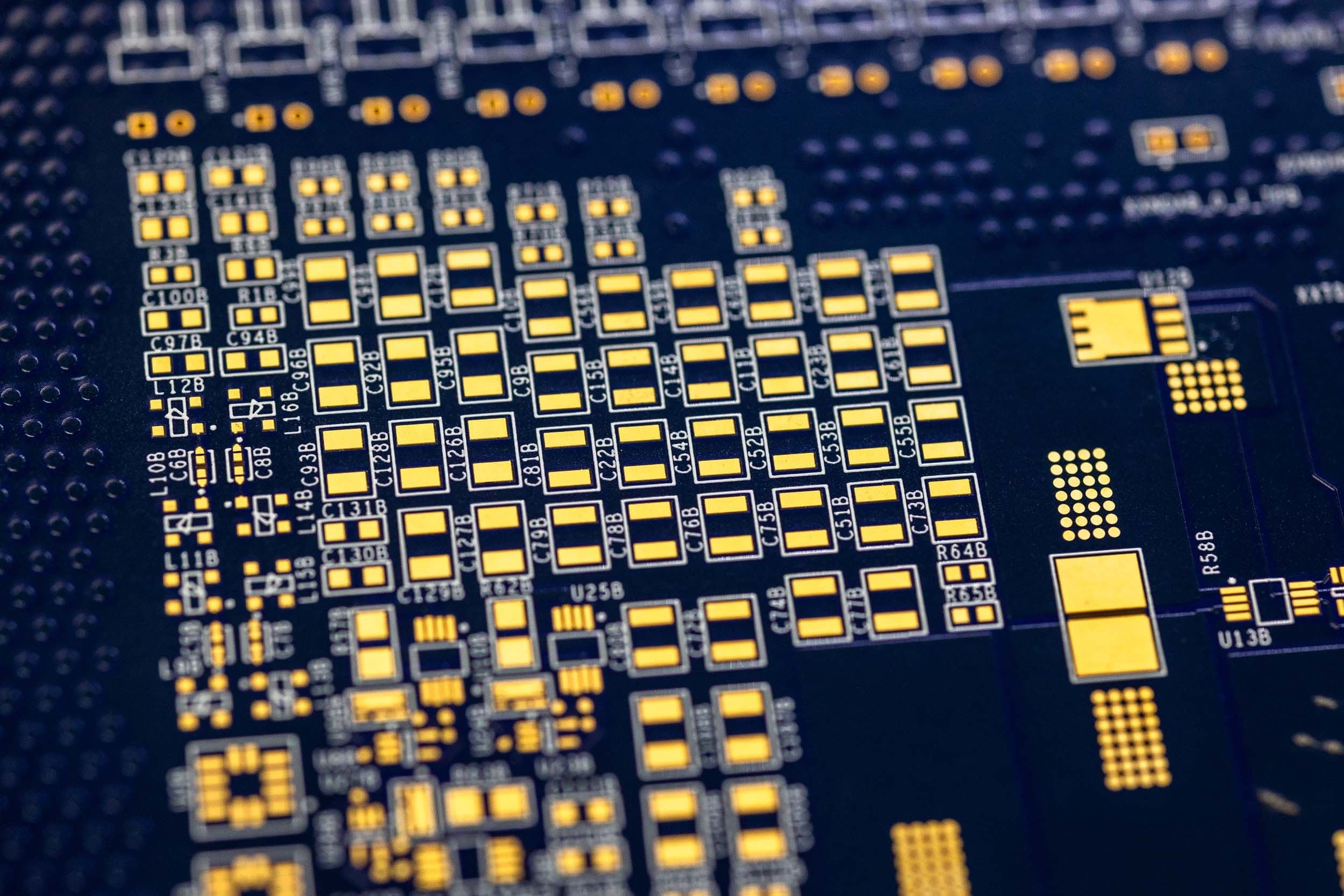
High-density interconnect PCBs for fine features, microvias, and complex multilayer designs, manufactured using production-ready processes with full engineering oversight to ensure reliable and repeatable fabrication of the most demanding constructions.
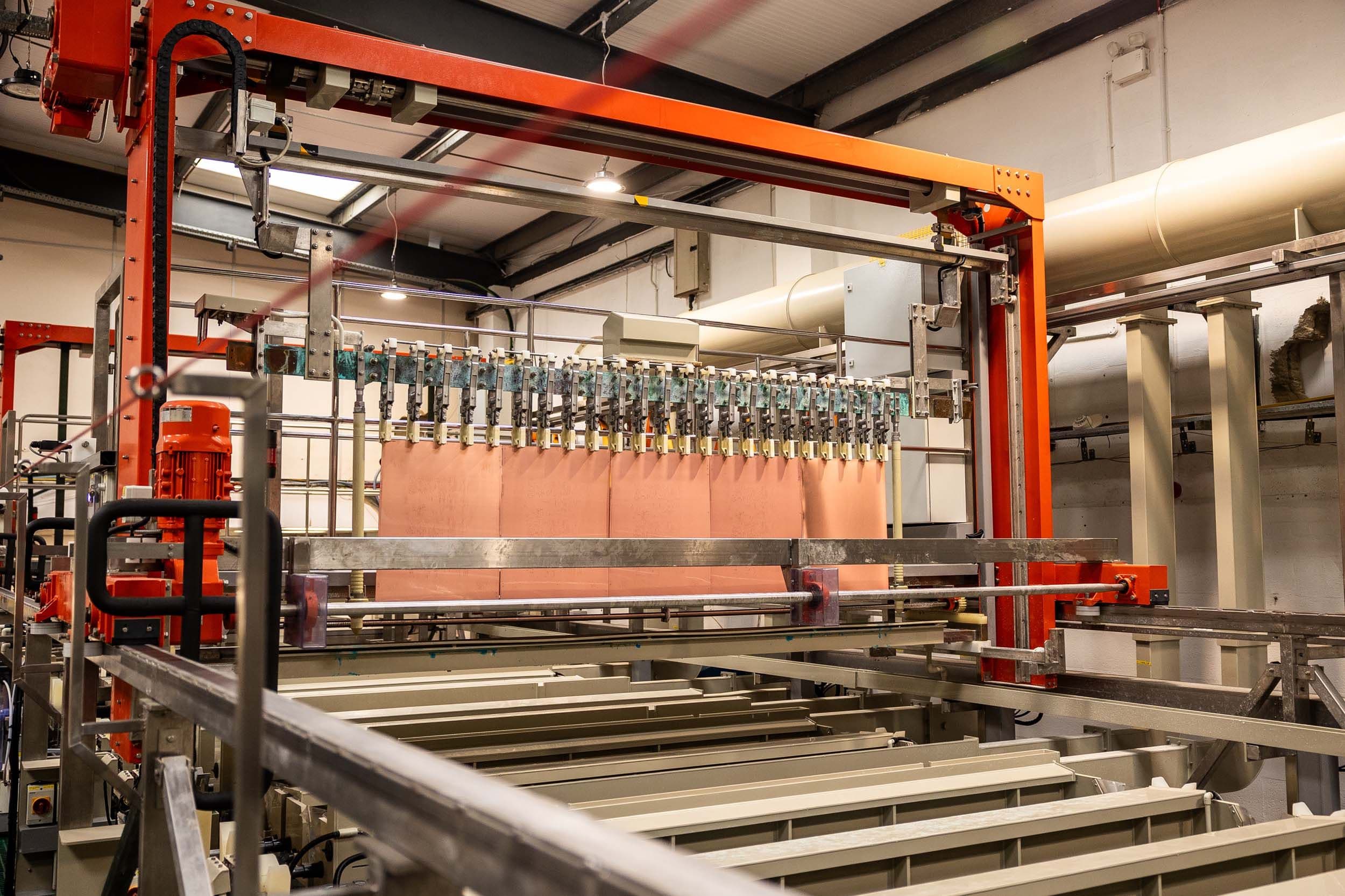
Copper via filling for blind, buried, and through-hole vias, supporting HDI constructions, via-in-pad designs, and thermally demanding multilayer PCBs where electrical continuity, thermal performance, and consistent fill quality are required.
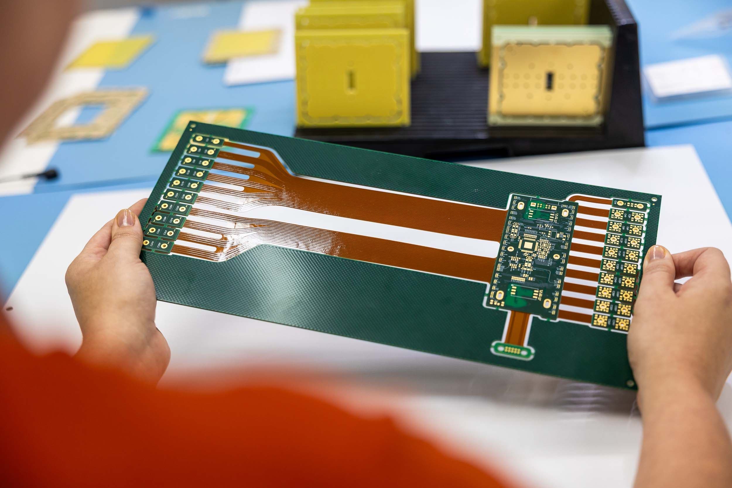
Complex flex and rigid-flex PCB constructions for space-constrained and dynamic applications, built with reliability and repeatability in mind to support confident integration where weight, form factor, or movement are critical.
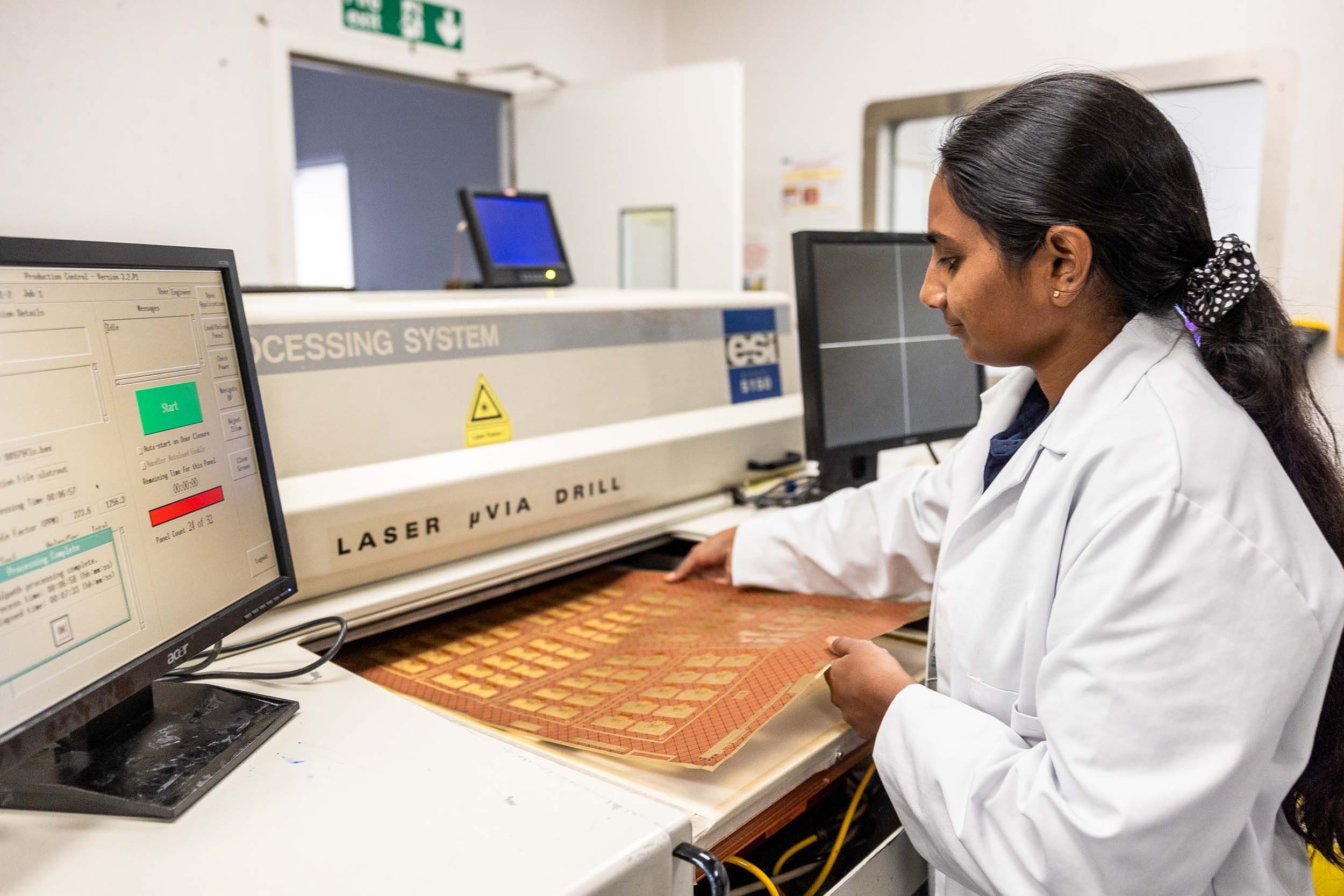
Support for specialist and hybrid PCB materials selected to meet thermal, electrical, and environmental performance requirements in applications where standard FR4 or conventional laminate systems cannot deliver the required performance.
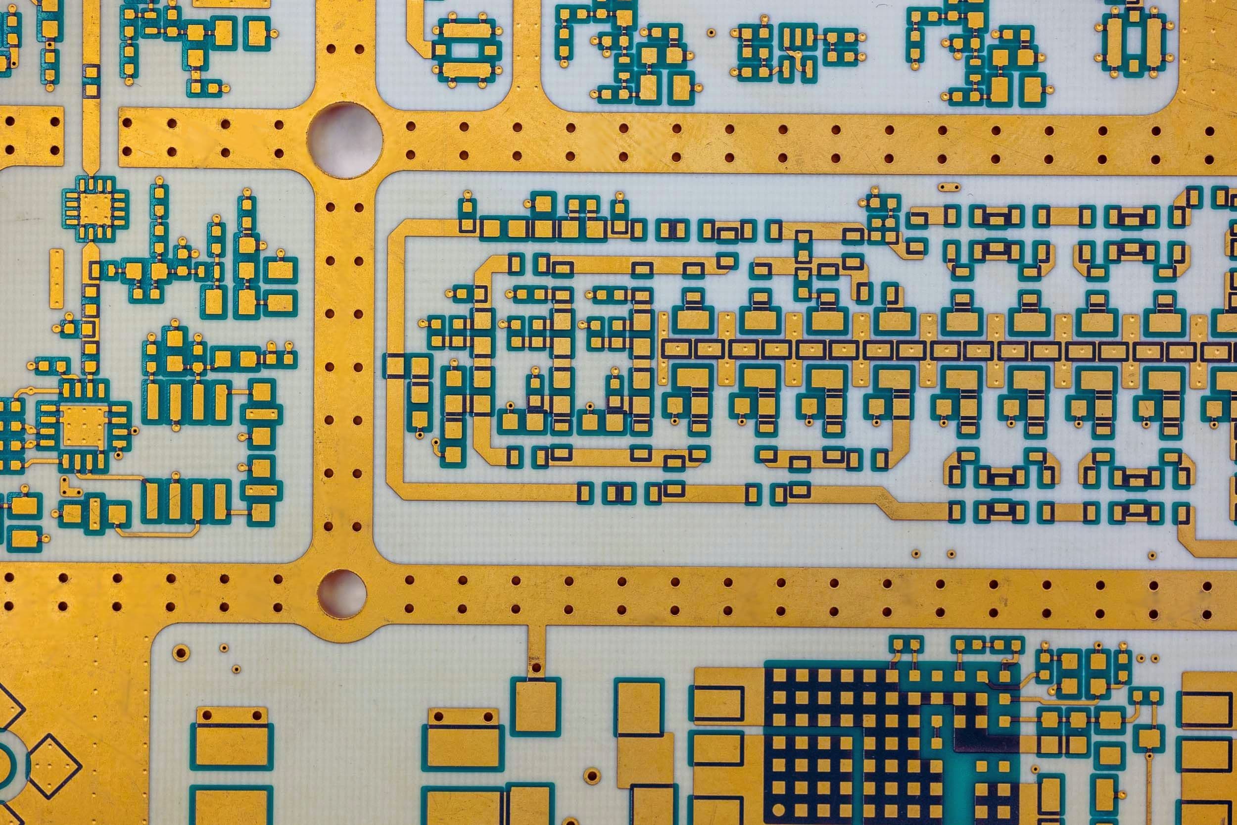
RF and high-frequency PCBs built to support controlled impedance, low-loss materials, and consistent signal integrity in demanding applications where dielectric performance, layer registration, and material choice directly affect circuit behaviour.