
PCB Technical Capabilities
A practical guide to our PCB manufacturing capabilities, tolerances, materials, and processes. Use it to qualify Exception PCB as a supplier, review design requirements, and prepare projects for manufacture.
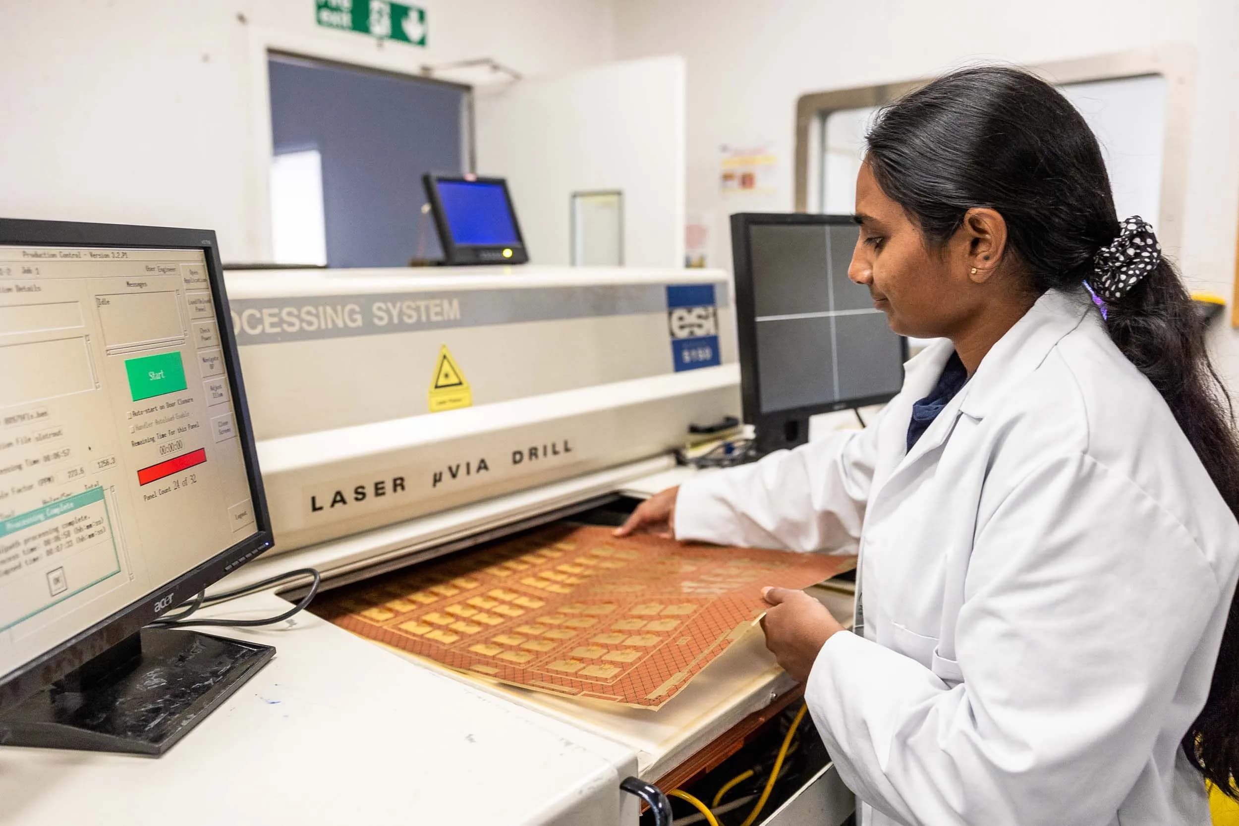
Engineering-led PCB material selection and processing, supporting electrical, thermal, mechanical, and RF performance in complex and high-technology multilayer designs.
Material selection influences far more than cost or availability. In high-performance electronics, the laminate system directly affects electrical behaviour, thermal stability, manufacturability, and long-term reliability. Exception PCB supports a broad range of PCB material families, from conventional FR4 systems through to polyimide, PTFE, and hybrid RF constructions.
Our engineers work closely with design teams to evaluate and select the most suitable material based on electrical and mechanical behaviour, stack-up design, process compatibility, and end-use operating conditions. We focus on what each material does in practice, not just what the datasheet says, ensuring the chosen system is manufacturable, reliable, and repeatable in production.
Find answers on via geometries supported, planarisation tolerances, resin fill consistency, and stack-up compatibility.
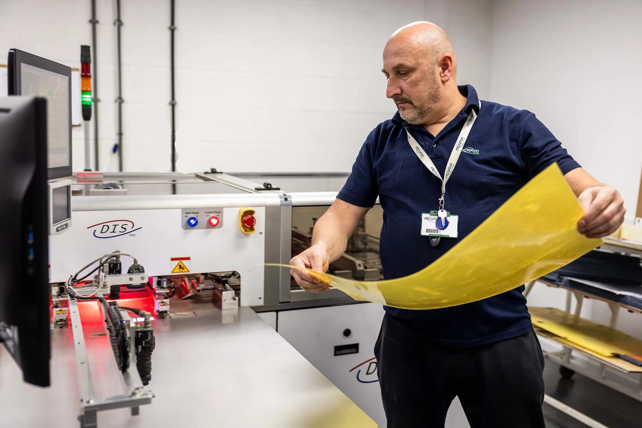
PCB material choice affects how a design performs throughout manufacture, assembly, and operational life.
Small differences in dielectric behaviour, thermal expansion, or mechanical stability can influence impedance consistency, solder joint reliability, or dimensional control within the finished PCB.
MATERIAL SELECTION BECOMES INCREASINGLY IMPORTANT WHEN DESIGNS INVOLVE:
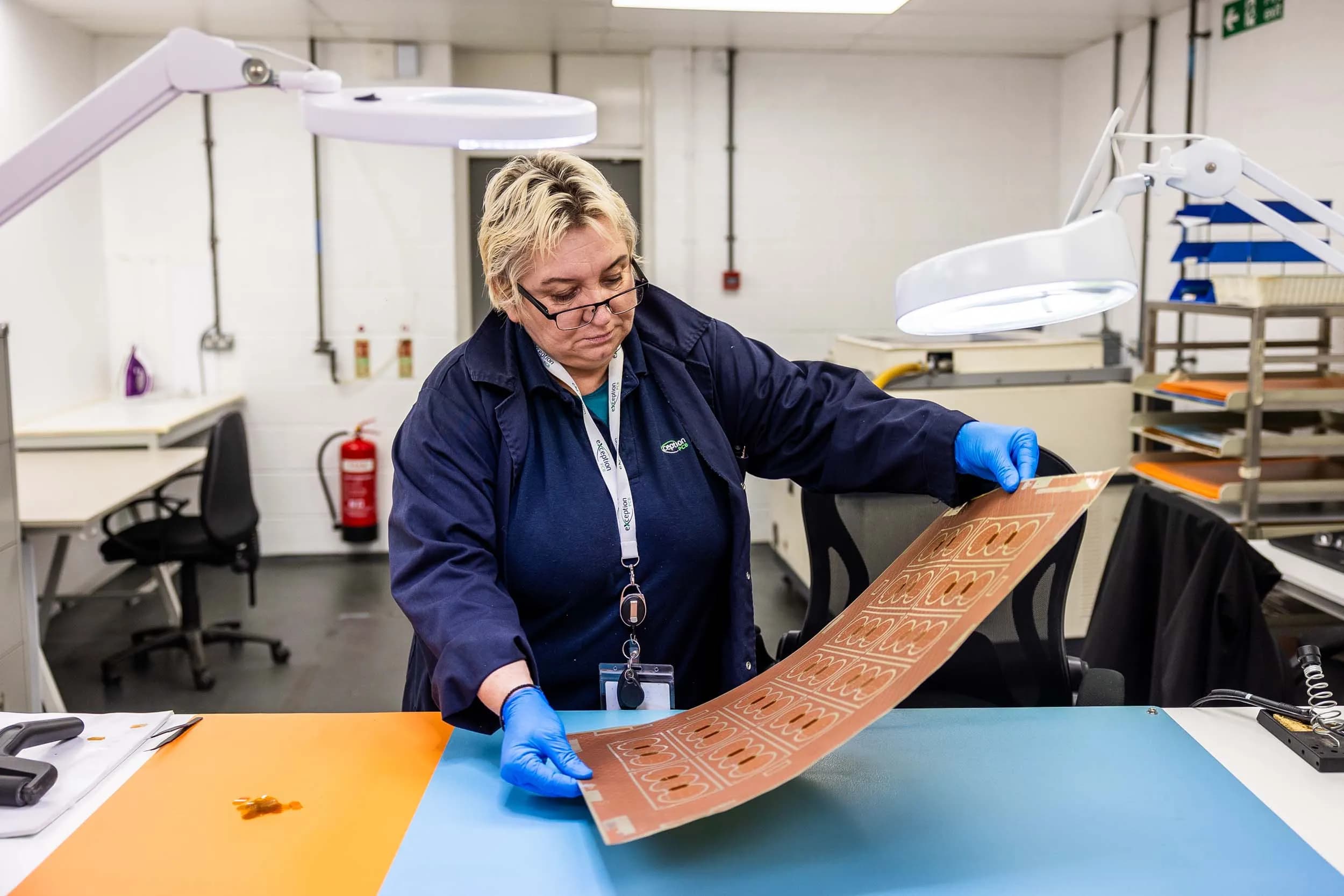
Engineers often evaluate materials not by brand name, but by how they perform within the intended application.
MATERIAL SELECTION DIRECTLY INFLUENCES:
At Exception PCB, material choice is considered alongside manufacturability to ensure performance targets remain achievable in production.
READY TO DISCUSS YOUR MATERIAL REQUIREMENTS?
Our engineers can help evaluate material options against your electrical, thermal, and mechanical requirements and confirm compatibility with your stack-up design
Advanced PCB manufacturing often requires multiple material systems depending on performance objectives. Exception PCB supports a range of laminate families selected to align with electrical, thermal, and mechanical requirements.
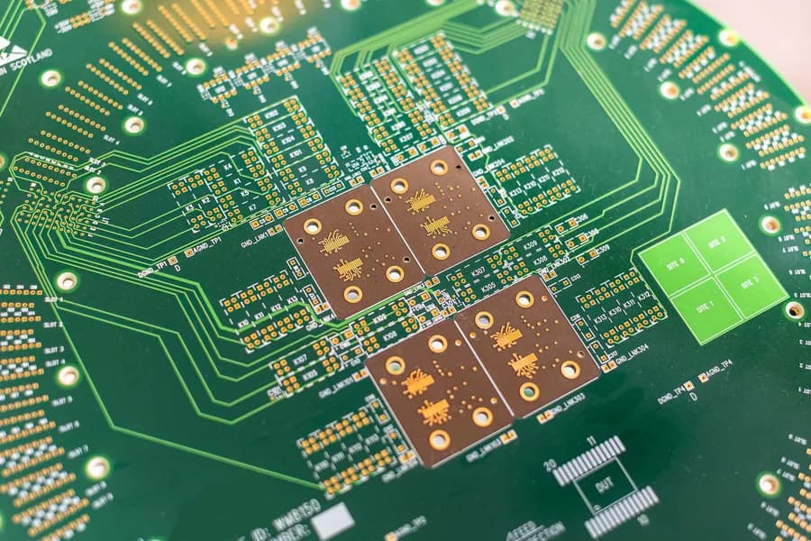
FR4 remains one of the most widely used PCB materials due to its balance of manufacturability, cost, and performance. Exception PCB supports enhanced high-Tg FR4 materials for a wide variety of applications.
FR4 SYSTEMS ARE COMMONLY USED FOR:
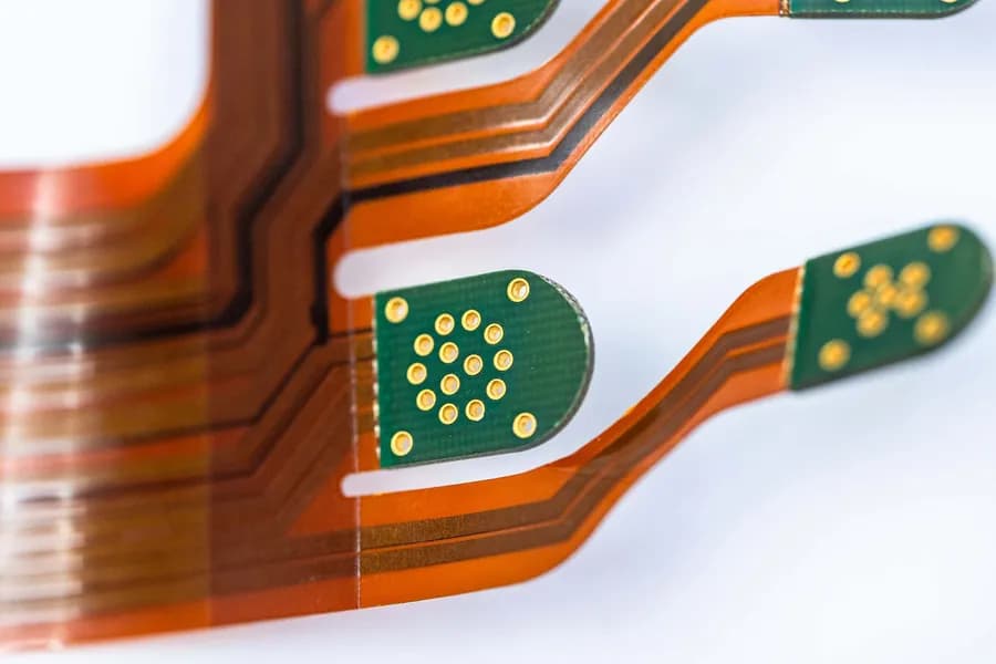
Polyimide materials are selected where elevated temperature resistance, mechanical durability, or long-term reliability are critical.
These materials perform well in environments where thermal cycling, vibration, or prolonged operating stress would challenge standard laminate systems.
Polyimide is commonly used within:
Polyimide structures offer improved dimensional stability and maintain performance across demanding operating conditions.
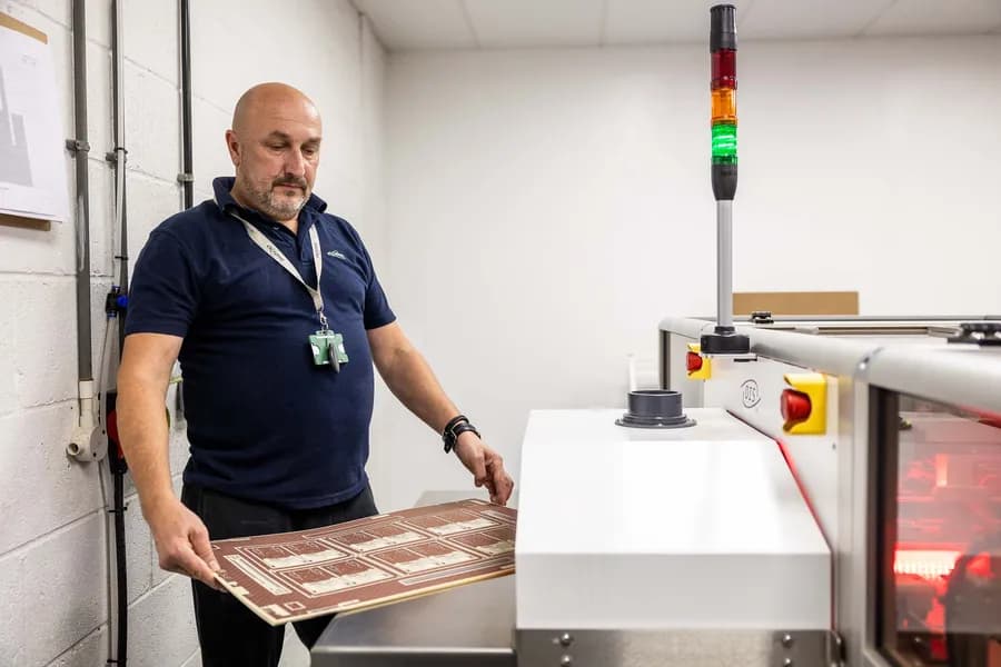
RF and microwave PCB designs require materials with predictable dielectric behaviour and low signal loss. Exception PCB supports PTFE-based and ceramic-filled laminates used where signal integrity and insertion loss become critical design considerations.
RF MATERIALS ARE COMMONLY USED FOR:
These materials require tighter process control during drilling, routing, lamination, and plating due to their unique mechanical behaviour.
To improve the cost and manufacturability Exception PCB can also provide alternatives to PTFE and ceramic filled materials that have similar performance properties.
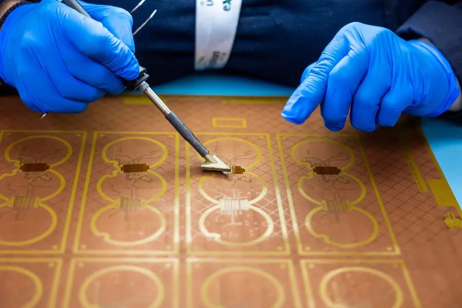
Many advanced designs require more than one material family within the same PCB structure. Hybrid stack-ups combine materials such as FR4, polyimide, and RF laminates to optimise electrical performance while controlling cost and complexity.
HYBRID CONSTRUCTIONS ARE COMMONLY USED WHERE:
Mixed-material stack-ups introduce additional manufacturing complexity because different material systems expand at different rates.
Lamination profiles must be selected to ensure all materials are fully cured without exceeding the property limits of the most thermally sensitive material in the build, and stack-ups must be kept symmetrical to avoid bow and twist.
Material performance is typically evaluated through behaviour and internal testing rather than just the manufacturers data sheets.
At Exception PCB, our technical engineering review process works closely with customers and their designs to focus on the material characteristics that influence manufacturing stability, reliability, and electrical performance.
Tg indicates the temperature range at which a material transitions from a rigid, stable state to a softer condition where its mechanical and thermal properties begin to change.
Higher Tg materials generally provide improved dimensional stability, thermal resistance, and reliability during PCB assembly, thermal cycling, and operational use.
These properties influence signal propagation, impedance behaviour, and transmission loss within the PCB structure. Lower Df materials are typically preferred for RF and high-speed digital applications where insertion loss and signal attenuation must remain controlled over longer transmission paths or at higher frequencies.
CTE defines how much a material expands and contracts during heating and cooling cycles.
Differences in CTE between material systems, copper, and PCB structures can influence via reliability, layer-to-layer registration, dimensional stability, and overall lamination performance during manufacture and thermal cycling.
Td indicates the temperature at which the resin system begins to chemically decompose and experience measurable material breakdown or weight loss.
Higher Td materials generally provide improved resistance to thermal degradation during high-temperature assembly processes and demanding operating conditions, helping maintain long-term material integrity and reliability.
Mechanical performance influences drill quality, dimensional control, flex durability, and multilayer registration throughout the manufacturing process.
Material stability becomes increasingly important in HDI, sequential lamination, and complex multilayer designs where tighter tolerances and repeated thermal processing place greater demands on the PCB structure.
Material thermal conductivity influences how efficiently heat is transferred through the PCB structure.
This becomes increasingly important in power electronics, RF systems, LED applications, and densely packaged assemblies where effective thermal management is critical to long-term reliability and performance.
Outgassing refers to the release of trapped gases, moisture, or volatile compounds from a material when exposed to elevated temperatures or vacuum environments.
Low outgassing materials are often preferred in aerospace, vacuum, high-reliability, and thermally demanding applications where contamination, material stability, and long-term performance must remain controlled.
Dielectric strength defines a material’s ability to withstand electrical stress without breaking down or allowing electrical conduction through the insulation system.
Higher dielectric strength materials provide improved electrical insulation performance and are important in high-voltage, power electronic, and high-reliability PCB applications.
Material behaviour changes depending on the PCB construction method. Not all laminates respond equally to drilling, lamination, or copper deposition. Exception PCB evaluates compatibility across advanced manufacturing processes.
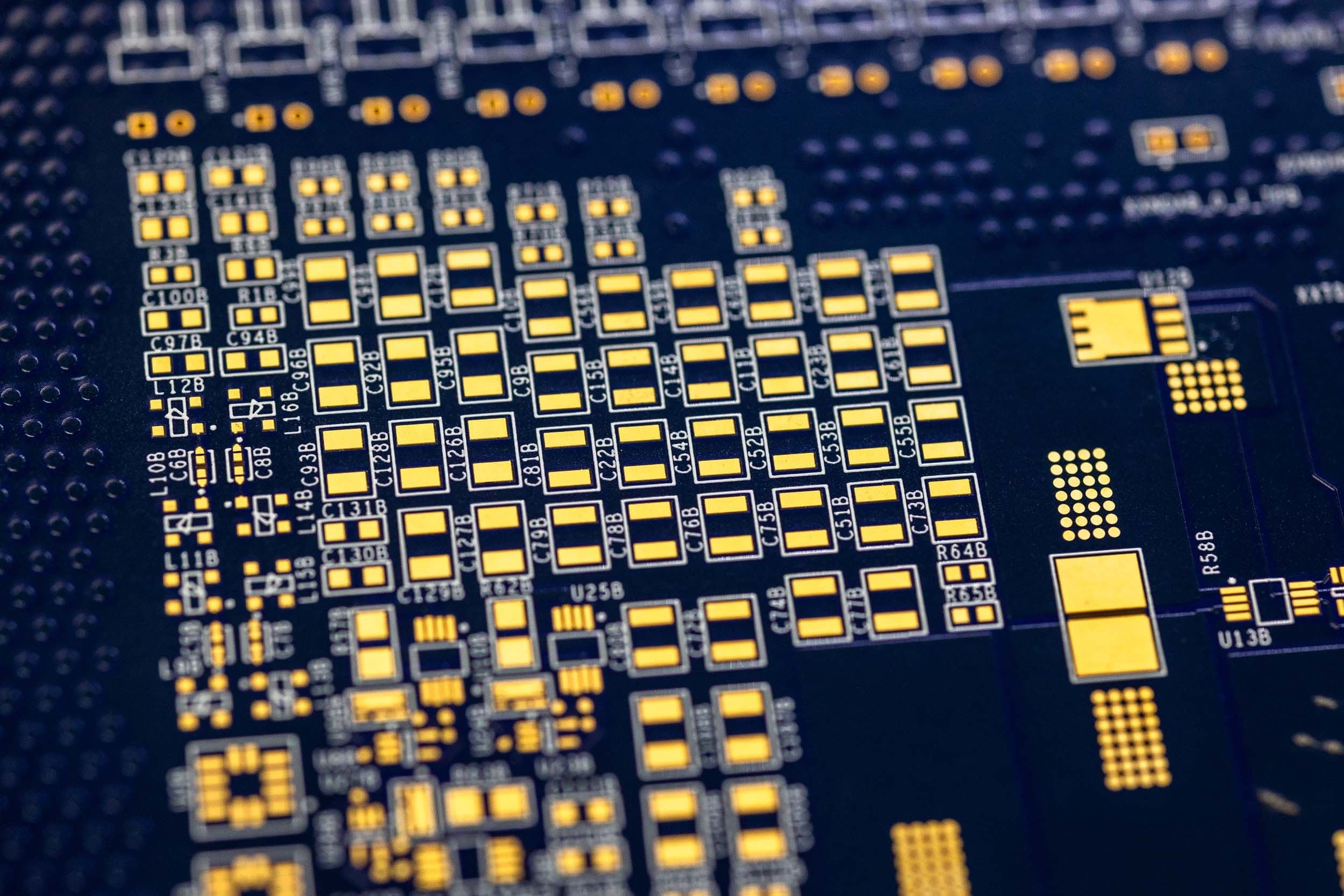
Sequential lamination and microvia formation place additional demands on dielectric stability and registration.
Material behaviour must remain predictable through multiple bonding cycles.
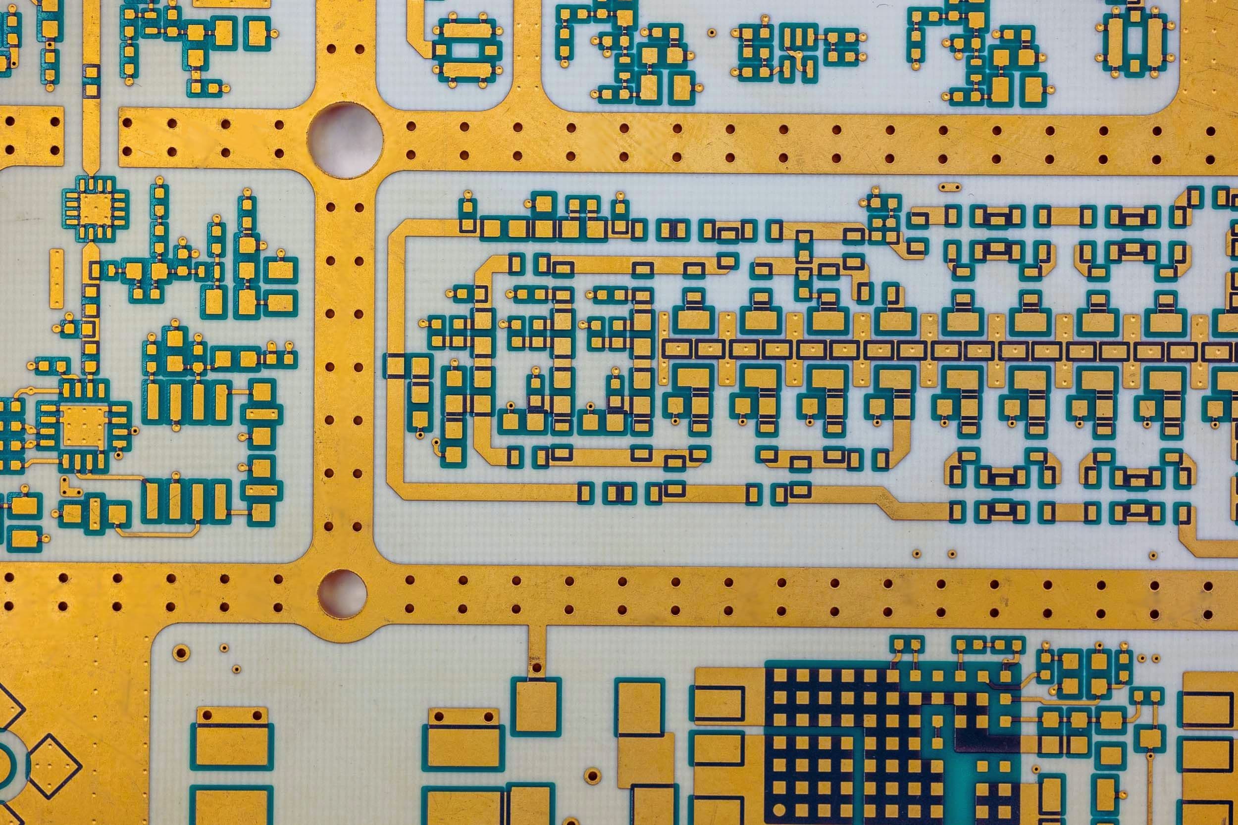
Dielectric consistency, copper roughness, and laminate stability influence insertion loss and impedance performance.
RF materials often require tighter process control to maintain high performance and signal integrity.
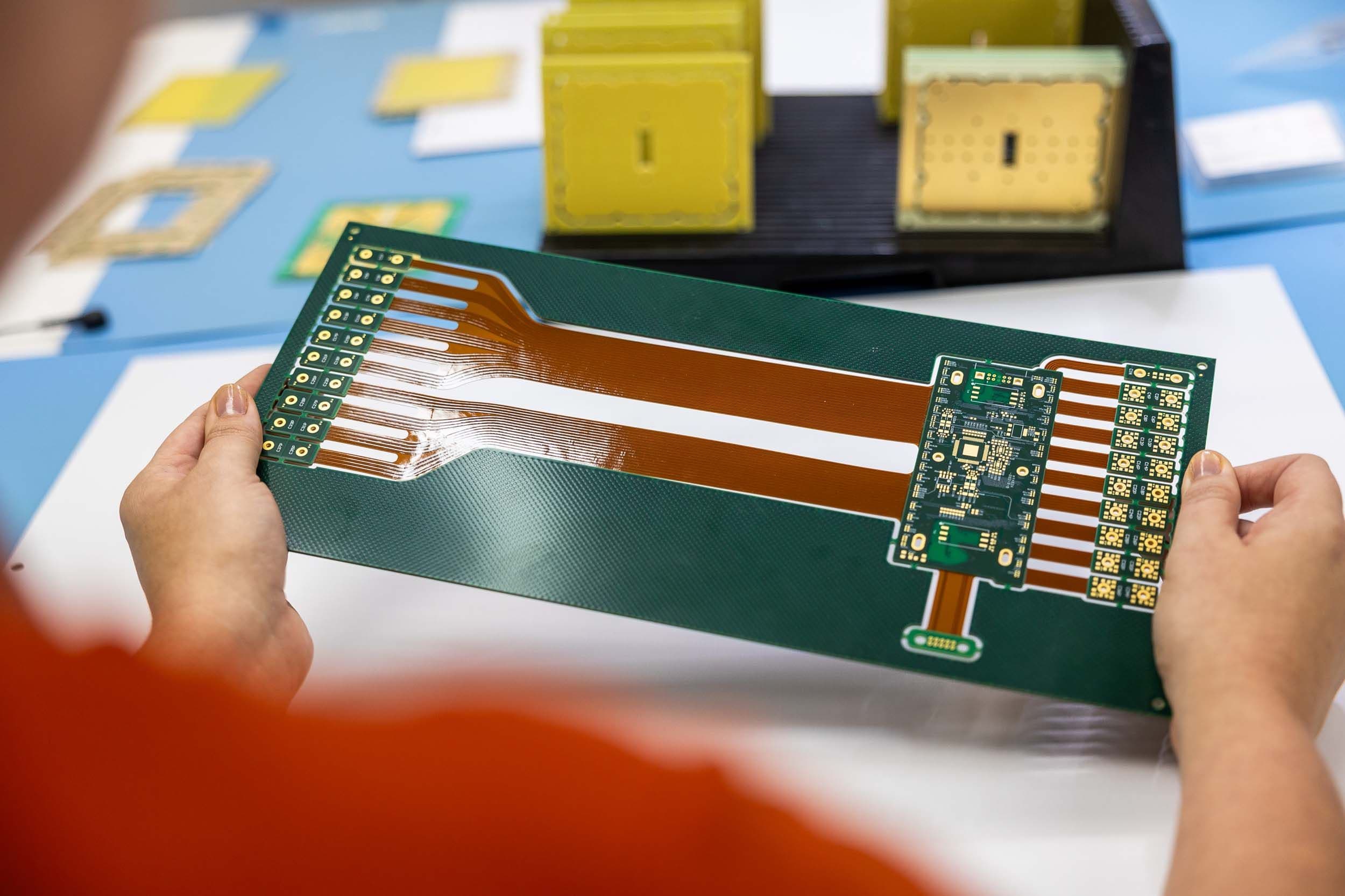
Flex constructions require materials capable of repeated movement without fatigue.
Polyimide systems with RA copper (rolled annealed) are commonly selected where bend performance and durability are essential.
EVALUATING MATERIALS FOR YOUR DESIGN?
Our engineers can help you select the right laminate for your stack-up and application, from standard FR4 alternatives through to PTFE-based, ceramic-filled, and hybrid constructions.
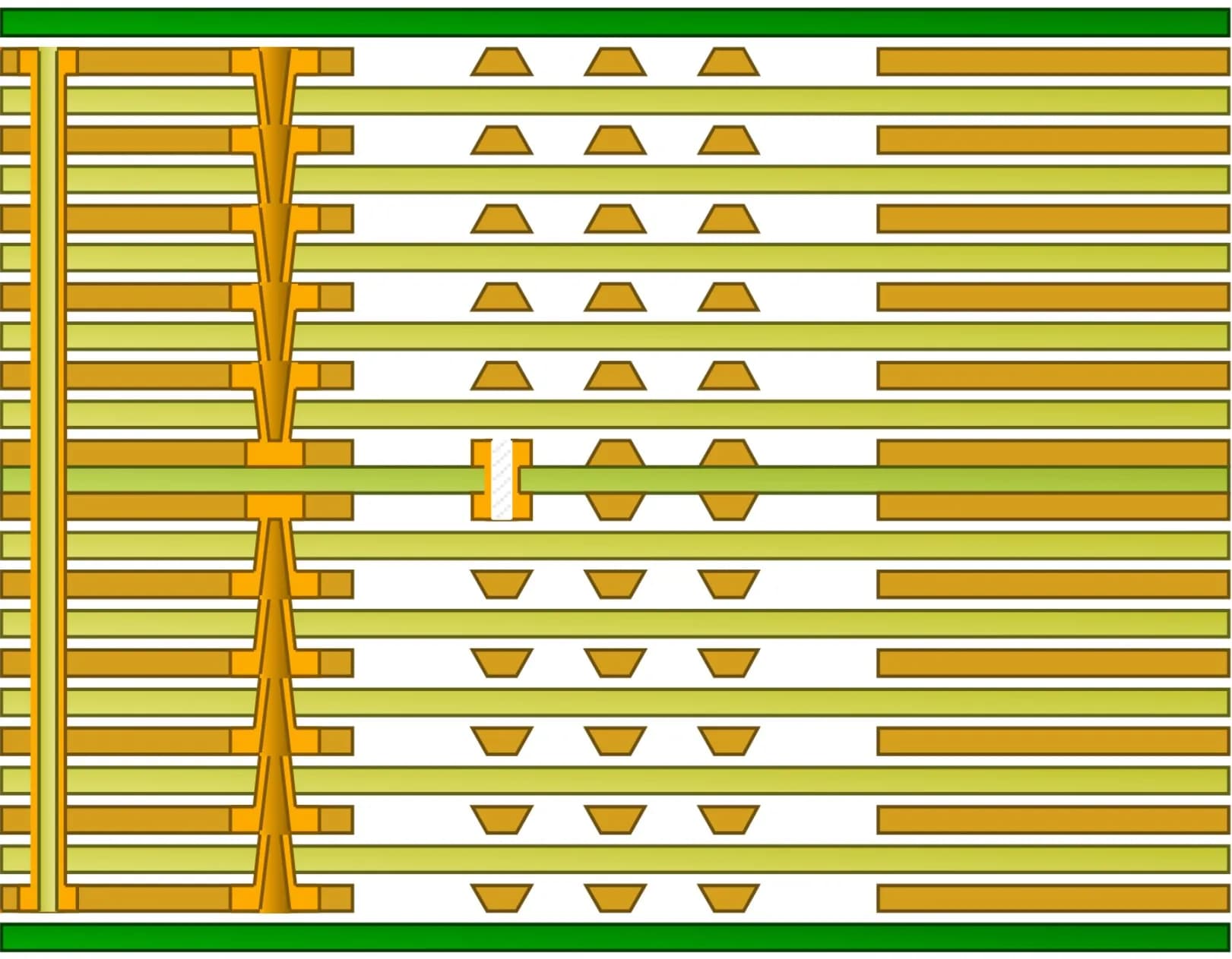
Cross-section illustration of a multilayer PCB stack-up showing copper layer construction, dielectric separation, and via interconnection structures across the layer sequence.
Stack-up design determines how materials behave collectively within the finished PCB.
Exception PCB supports engineering-led stack-up planning to ensure material systems remain aligned with electrical and manufacturing objectives. Our engineering process also includes impedance calculations to ensure the design requirements are met.
Stack-up planning considers:
The objective is to ensure the finished PCB performs consistently throughout manufacture and operational life.
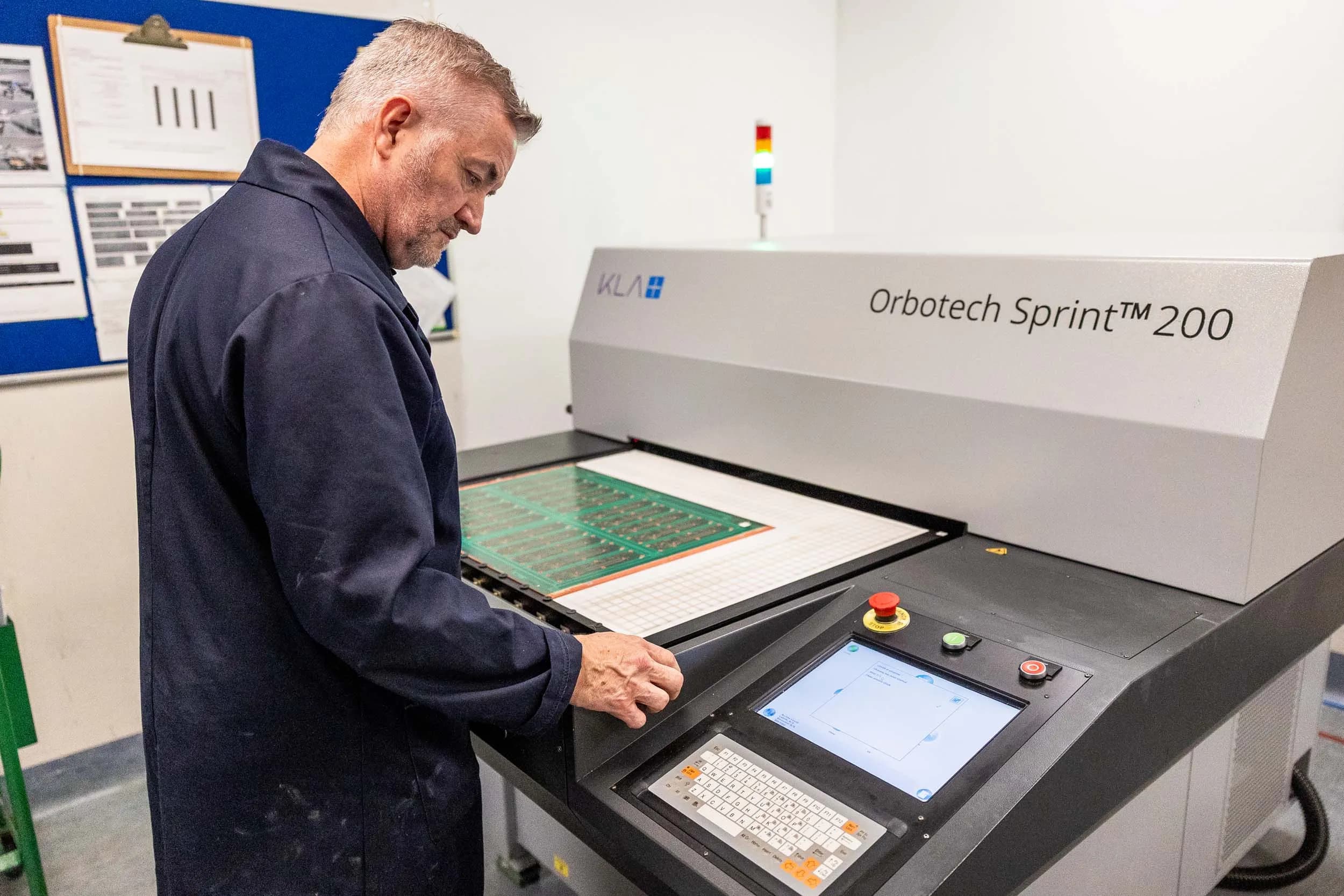
Advanced materials require tighter process control than standard PCB constructions.
Exception PCB integrates verification throughout manufacture to ensure material behaviour remains stable and repeatable.
QUALITY CONTROL INCLUDES:
These controls support repeatability across R&D, NPI, and production batches.
Material selection often involves trade-offs between performance, manufacturability, availability, and cost.
Exception PCB works closely with design teams to ensure the selected material system supports both design intent and stable production.
MATERIAL SELECTION SUPPORT INCLUDES:
TALK TO OUR ENGINEERS
Whether you are evaluating RF laminates, hybrid stack-ups, or high-temperature materials, our engineers are happy to share their material knowledge.
Below we have answered the questions our engineers are asked most often. If yours isn't covered, get in touch with the team directly.
Material selection depends on how the PCB will perform electrically, thermally, and mechanically within the finished product.
PCB designers usually need to evaluate:
If you need help with choosing the right material for your project, please contact our engineering team.
Polyimide materials are commonly recommended when the application requires increased thermal resistance or long-term mechanical stability. Typical glass transition temperature (Tg) of polyimide substrates is around 250°C.
They are often used in:
Polyimide materials maintain structural integrity under conditions that may exceed the performance range of standard FR4.
PTFE and materials with ceramic fillers are selected where signal loss, dielectric stability, and impedance consistency become critical.
PTFE-based laminates and ceramic-filled RF materials typically offer:
These materials are commonly used in radar, communications, sensing, and microwave applications.
Yes. Hybrid stack-ups are commonly used when different sections of the PCB require different performance characteristics.
For example:
Hybrid constructions help optimise electrical performance while managing cost and manufacturability.
Material properties directly influence impedance behaviour.
Dielectric constant (Dk), dielectric thickness, and copper geometry all contribute to how signals propagate through the PCB.
Changes in material consistency can affect:
Material selection is often reviewed together with stack-up design to ensure impedance targets remain achievable.
No. Some materials behave differently during drilling, lamination, or copper deposition.
HDI structures require materials that maintain:
Engineering review helps ensure material selection remains compatible with HDI manufacturing processes.
Mixed-material constructions can introduce differences in thermal expansion, lamination behaviour, and dimensional movement.
Without proper control, this may affect:
Exception PCB evaluates compatibility between materials during stack-up planning to minimise manufacturing risk.
Advanced materials often require additional process control and inspection.
Verification may include:
These checks confirm that the material system remains stable throughout manufacture.
Material selection should ideally be reviewed early in the design process.
Early engagement allows engineers to evaluate:
This reduces redesign risk and improves confidence before release to manufacture.
Explore guides and references covering PCB construction types, laminate properties, and the full range of manufacturing capabilities at Exception PCB.
Explore related technologies that depend on material selection, stack-up control and stable manufacturing processes across complex PCB designs.
RF and high-frequency PCBs built to support controlled impedance, low-loss materials, and consistent signal integrity in demanding applications where dielectric performance, layer registration, and material choice directly affect circuit behaviour.
Complex flex and rigid-flex PCB constructions for space-constrained and dynamic applications, built with reliability and repeatability in mind to support confident integration where weight, form factor, or movement are critical.
High-density interconnect PCBs for fine features, microvias, and complex multilayer designs, manufactured using production-ready processes with full engineering oversight to ensure reliable and repeatable fabrication of the most demanding constructions.
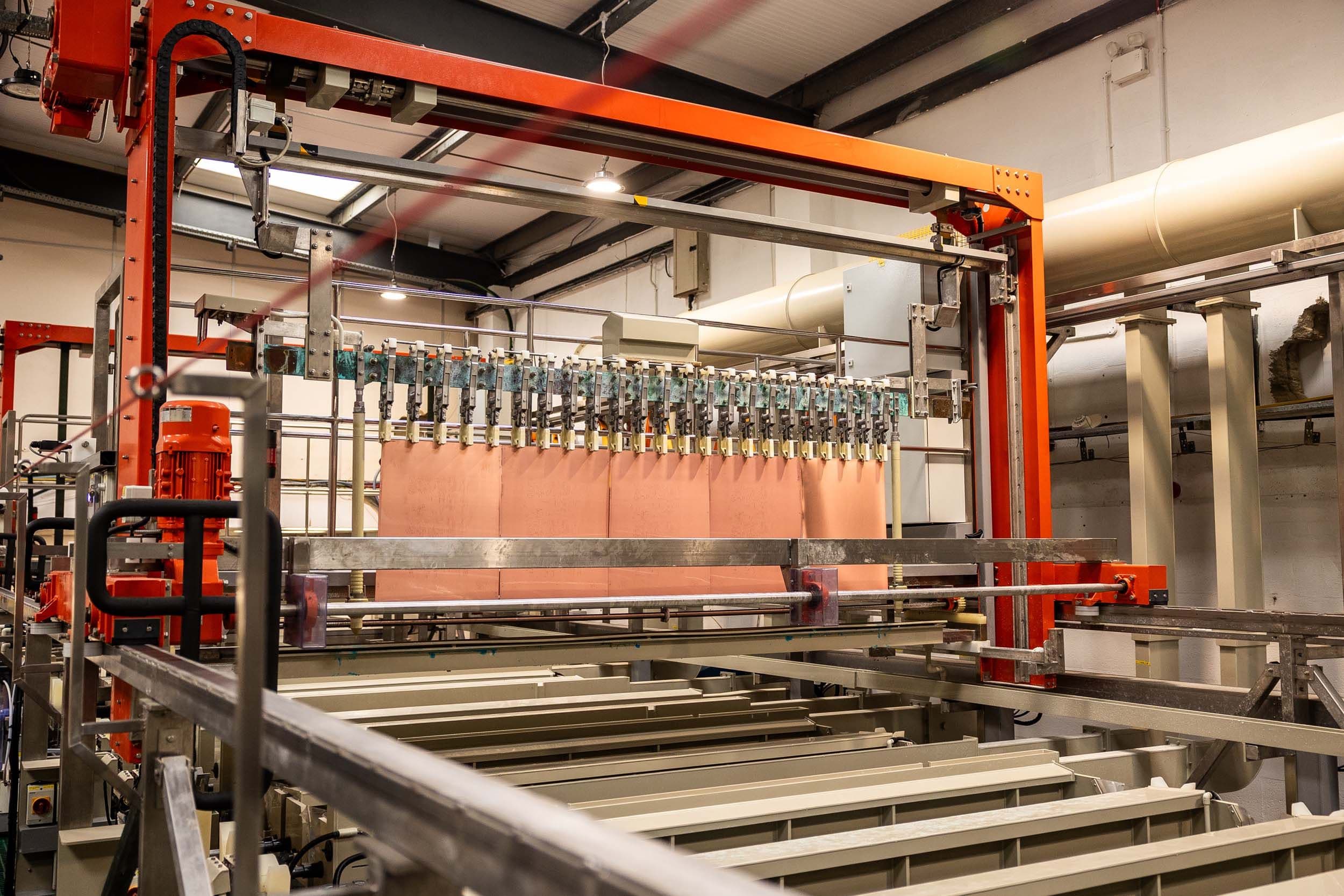
Copper via filling for blind, buried, and through-hole vias, supporting HDI constructions, via-in-pad designs, and thermally demanding multilayer PCBs where electrical continuity, thermal performance, and consistent fill quality are required.
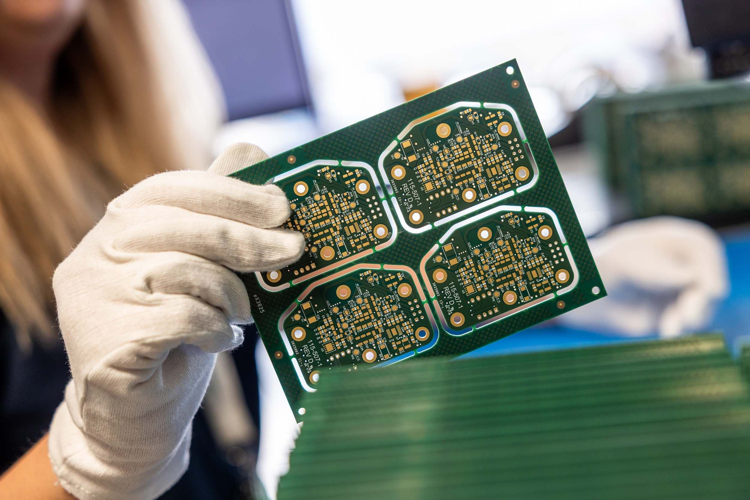
Resin via fill for blind, buried, and through-hole vias, providing consistent surface planarity to support via-in-pad designs, fine-pitch assembly, and sequential lamination builds where assembly quality and via integrity matter.