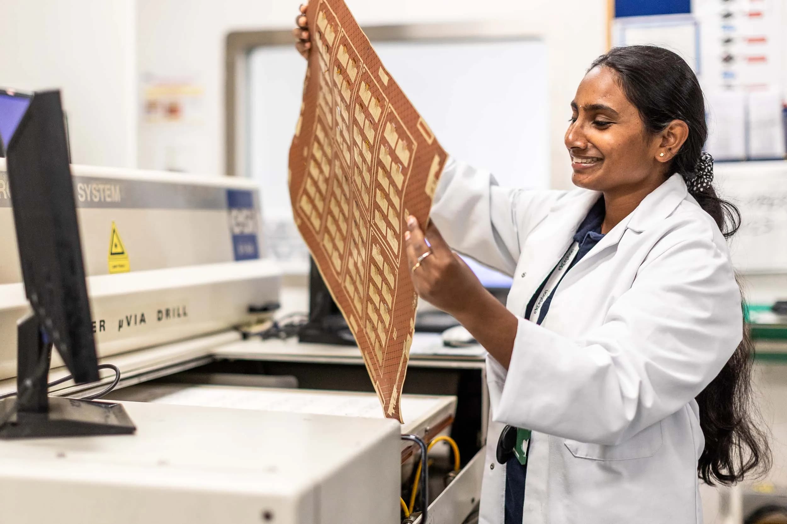
Side profile of a smiling Exception PCB engineer holding a flexible circuit sheet next to a micro via drill.

DESIGN FOR MANUFACTURE (DFM)

High-technology PCB manufacturing from our facility in Tewkesbury, combining rigorous process control, experienced engineers, and the resilience of UK supply-chain manufacture.

PCB DESIGN FOR MANUFACTURE REVIEW

Exception PCB provides DFM review embedded in the manufacturing process and as a standalone service for customers at earlier stages of development. Review is carried out by our in-house engineering team using In-Cam Pro, the industry-leading PCB layout analysis software.

Our engineers understand how PCBs behave in production, drawing on direct experience of lamination, drilling, plating, and inspection, and apply that knowledge to every review.

The service covers all PCB types, with particular specialism in HDI, flex, controlled impedance, and advanced material stack-ups.

LET OUR ENGINEERS REVIEW YOUR DESIGN

Whether you are preparing for prototype or moving into production, our team will confirm the right manufacturing route and identify any risks before your build begins.


TALK TO OUR ENGINEERS

WHAT OUR DFM REVIEW COVERS

DESIGN DATA INTAKE

We receive and validate design files, reviewing stack-up, layer count, finished board specification, and intended manufacturing route before analysis begins.

STACK-UP & MATERIAL REVIEW

Dielectric thicknesses, copper weights, and material selection are assessed to confirm suitability for the specified construction and manufacturing process.

DRILL & VIA STRUCTURES

Via aspect ratios, microvia depth, and hole-to-copper and hole-to-edge clearances are reviewed against process capability to confirm drill feasibility.

COPPER DISTRIBUTION

Copper distribution across all layers is assessed to confirm plating consistency and dimensional stability through lamination.

CONTROLLED IMPEDANCE

Controlled impedance requirements are reviewed against the proposed stack-up, with recommendations where geometry adjustment or tolerance tightening is needed.

TRACK & GAP

Minimum feature sizes are checked against manufacturing process capability. Any areas operating at or beyond process limits are flagged with context and severity.

RISK REPORT

All findings are documented in a clear risk report, prioritised by severity, with specific and actionable recommendations for each identified issue.

SIGN-OFF OR HANDOVER

Reviewed designs progress to manufacture or are returned with a full written report for the customer to act on.

TWO WAYS TO WORK WITH US

Exception PCB's DFM service is structured to support customers at different stages of their programme.

INTEGRATED DFM

For customers placing manufacturing orders with Exception PCB, DFM is embedded in the production workflow as standard. Before any board reaches the production floor, our engineering team reviews design data, confirms production intent, and identifies areas of risk.

There is no separate process to initiate and no additional step to request. It is part of how we manufacture.

STANDALONE DFM REVIEW

For customers at an earlier stage of development, DFM is available as a standalone service. This is suited to teams who want to validate designs before committing time and budget to production, whether at design freeze, pre-NPI, or during active development.

We provide a structured review and written report. No manufacturing order is required, and the service can be used as a one-off engagement or as part of an ongoing development programme.

An inspector's hands in white protective gloves holding a green multi-panel board layout beneath a digital microscope camera lens.

WHY EARLY DFM REVIEW MATTERS

Design errors that reach manufacture cost far more to resolve than those caught during review. For complex PCB programmes, the gap between a DFM change and a production re-spin can mean weeks of delay and significant additional expenditure.

Our engineering team works with customers to close that gap early. Customers typically benefit from:

  • Fewer design re-spins and shorter iteration cycles
  • Greater confidence when committing to tooling and production volume
  • Earlier identification of layout and stack-up issues
  • Faster NPI progression and more predictable programme timelines
  • Direct access to the engineers who carried out the review, so findings can be discussed and acted on

DFM FOR ADVANCED PCB TECHNOLOGIES

DFM review applies to all PCB construction types but delivers the greatest value for complex and advanced designs, where the consequences of a design-to-manufacture conflict are most significant.

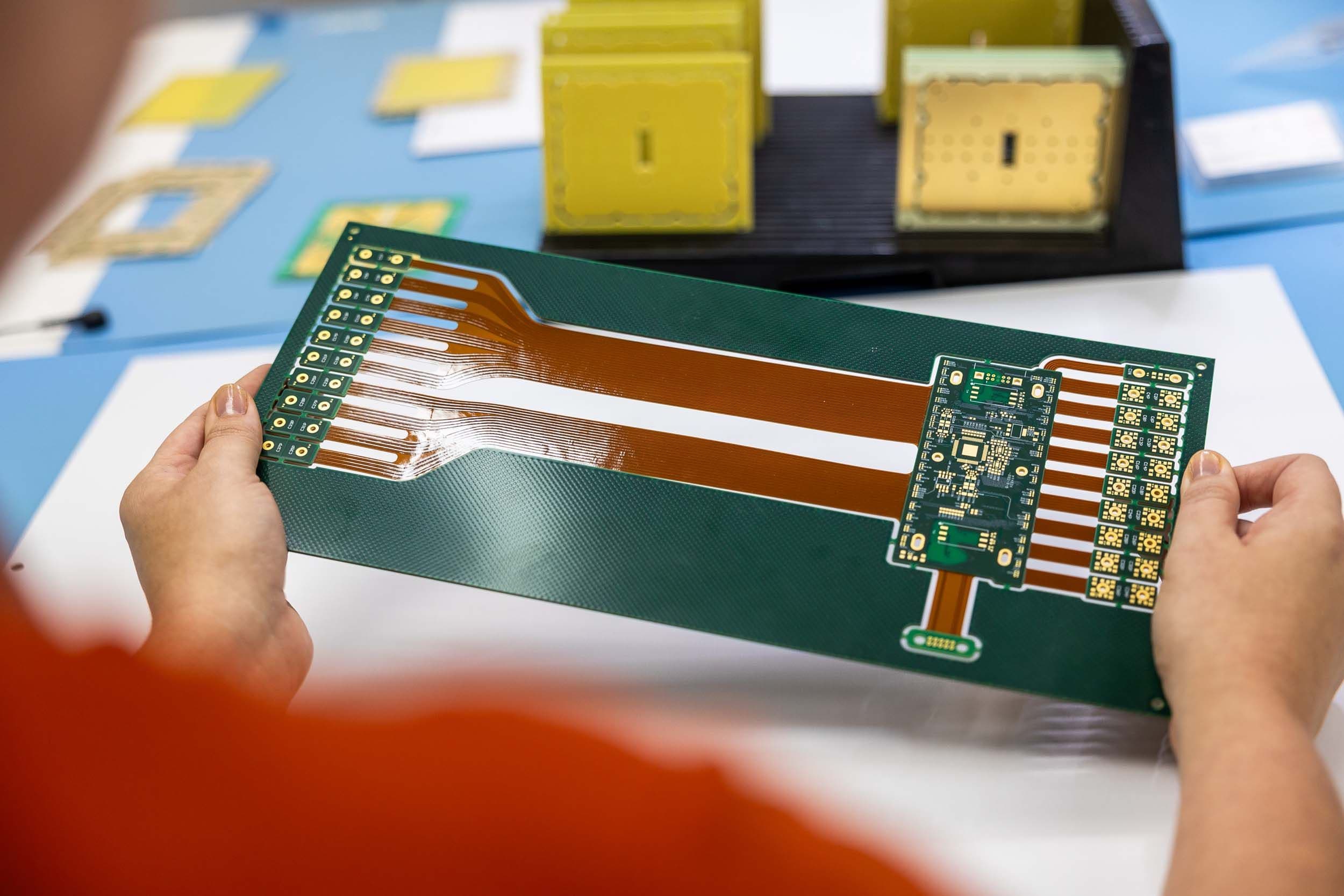
Technician holding a complex green rigid-flex circuit board panel with amber flexible interconnect extensions.

Flex & Rigid-Flex

Complex flex and rigid-flex PCB constructions for space-constrained and dynamic applications, built with reliability and repeatability in mind to support confident integration where weight, form factor, or movement are critical.

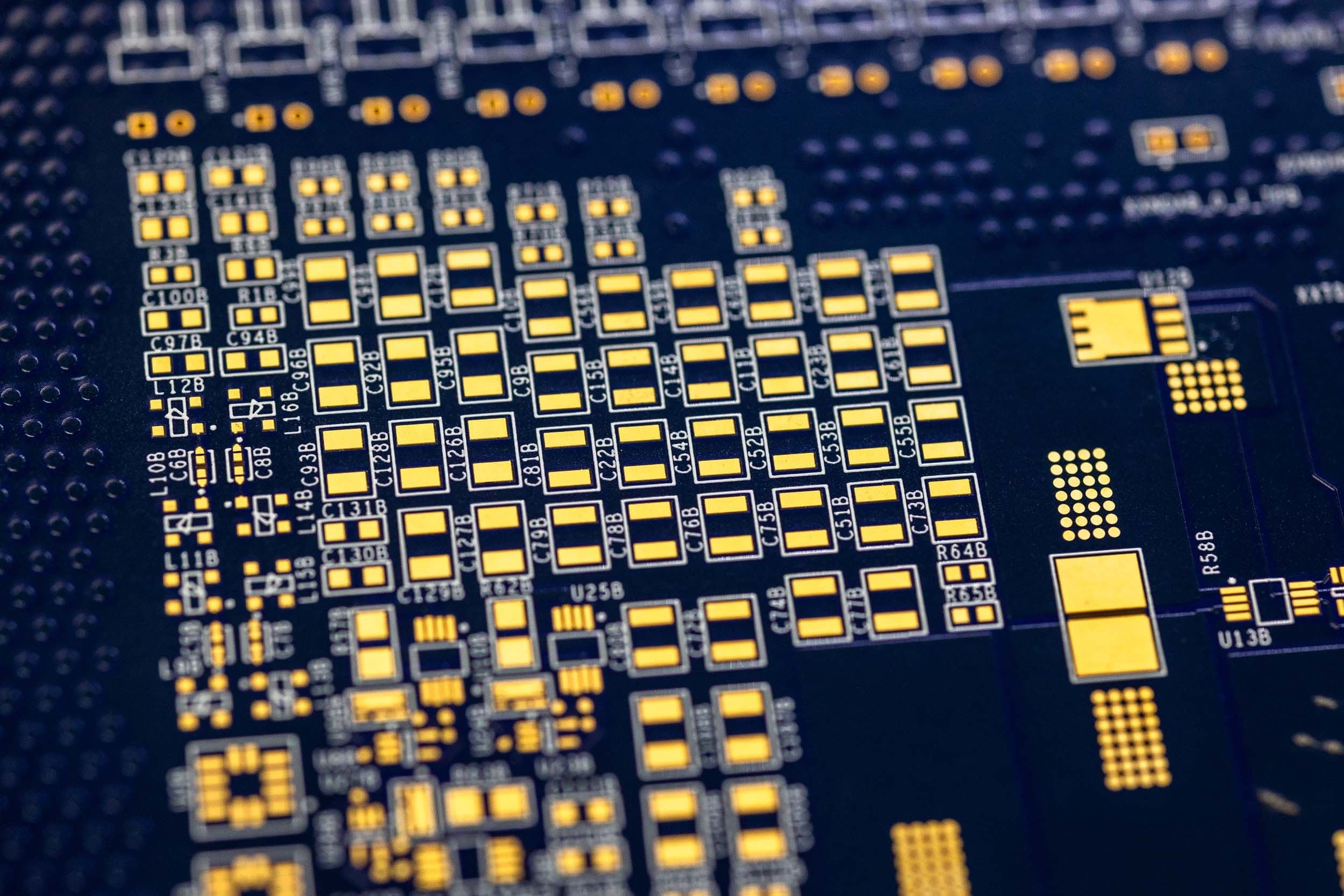
Macro view of a dark, high-density PCB showing precise gold pad layouts and trace routing.

HDI

High-density interconnect PCBs for fine features, microvias, and complex multilayer designs, manufactured using production-ready processes with full engineering oversight to ensure reliable and repeatable fabrication of the most demanding constructions.

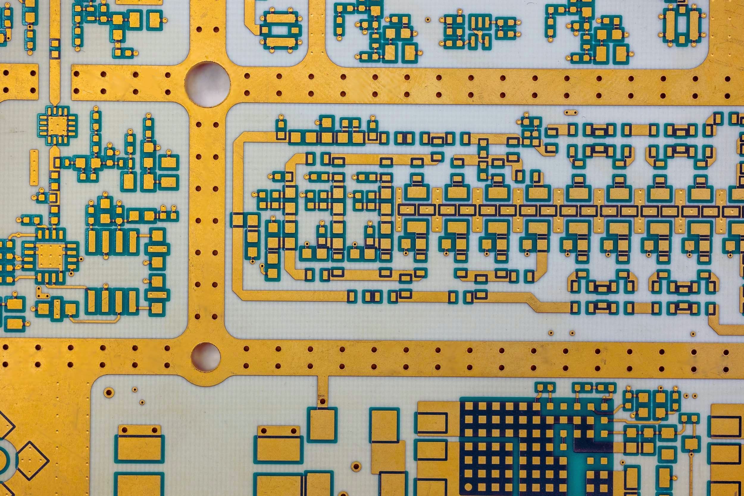
Macro close-up of ENIG gold-plated pads and precision circuit trace routing on a white substrate RF PCB, showing the surface finish quality and high-density layout of Exception PCB's RF manufacturing capability.

RF

RF and high-frequency PCBs built to support controlled impedance, low-loss materials, and consistent signal integrity in demanding applications where dielectric performance, layer registration, and material choice directly affect circuit behaviour.

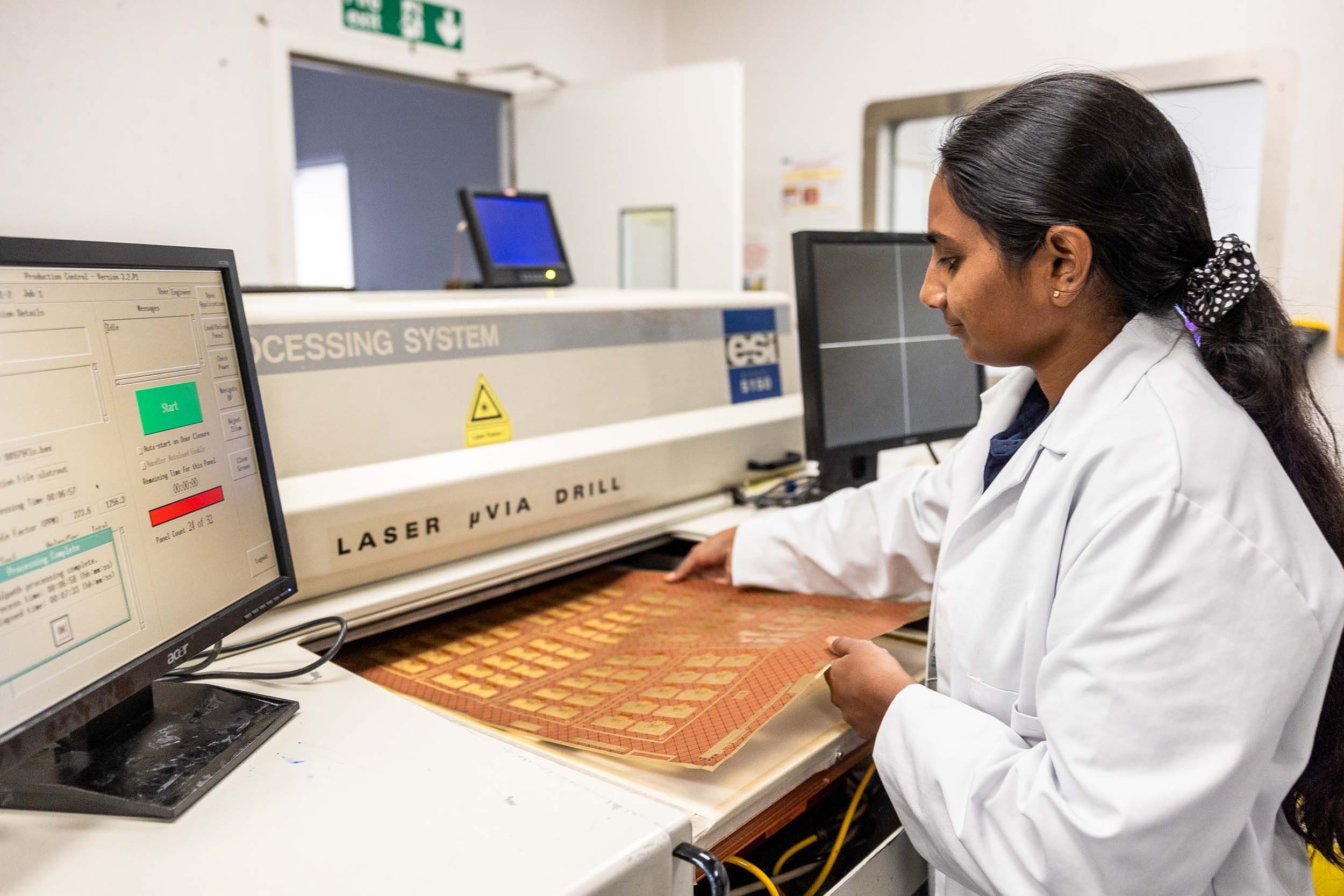
Exception PCB operator loading a flexible printed circuit board panel into an ESI laser micro via drill processing system.

Advanced Materials

Support for specialist and hybrid PCB materials selected to meet thermal, electrical, and environmental performance requirements in applications where standard FR4 or conventional laminate systems cannot deliver the required performance.

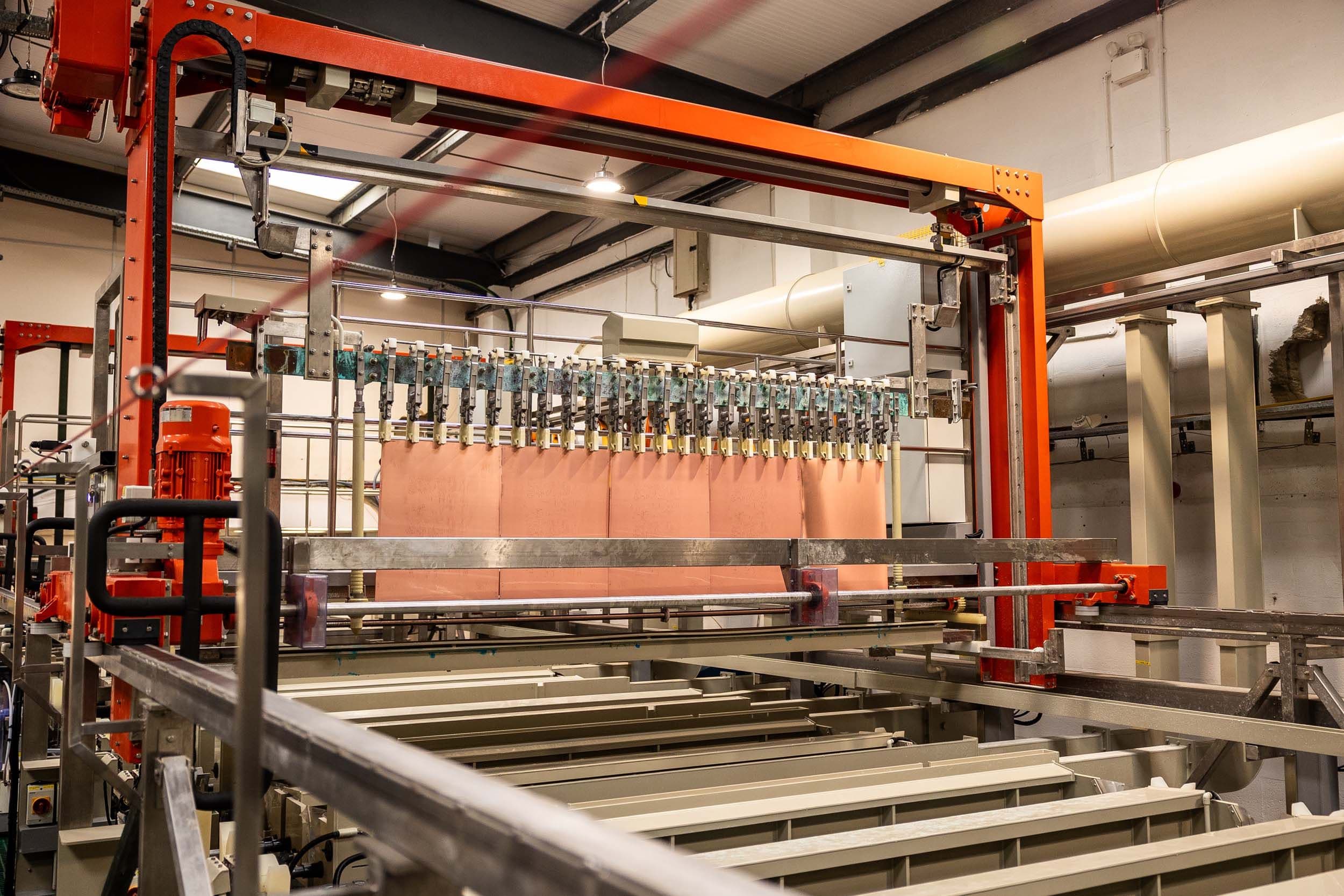
Wide landscape view of an automated electrochemical processing line inside the manufacturing plant.

Copper Via Fill

Copper via filling for blind, buried, and through-hole vias, supporting HDI constructions, via-in-pad designs, and thermally demanding multilayer PCBs where electrical continuity, thermal performance, and consistent fill quality are required.

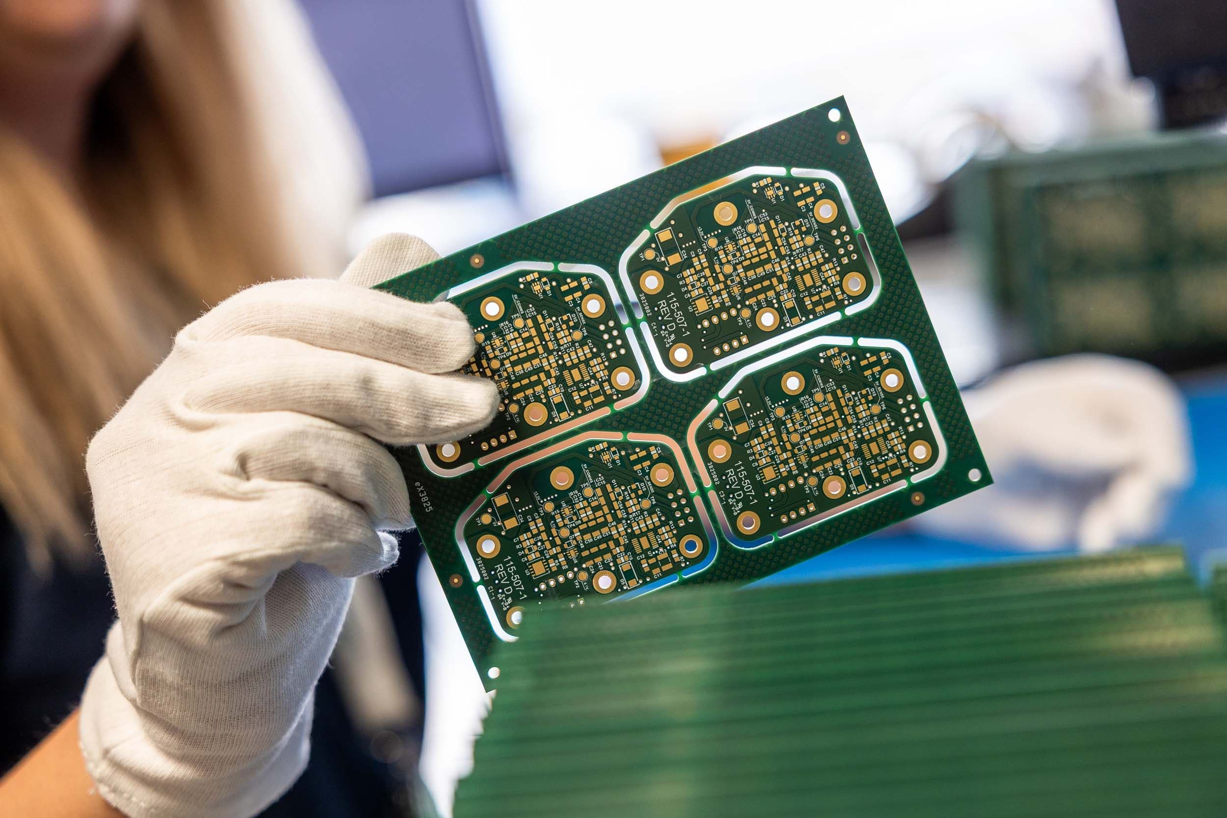
Exception PCB technician in a white glove holding a green printed circuit board panel with four individual circuits.

Resin Via Fill

Resin via fill for blind, buried, and through-hole vias, providing consistent surface planarity to support via-in-pad designs, fine-pitch assembly, and sequential lamination builds where assembly quality and via integrity matter.

READY TO DISCUSS YOUR DESIGN?

Whether you are at early design stage or preparing to move into production, our engineers are ready to support your programme.

RELATED ARTICLES

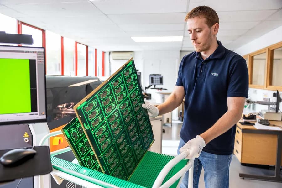
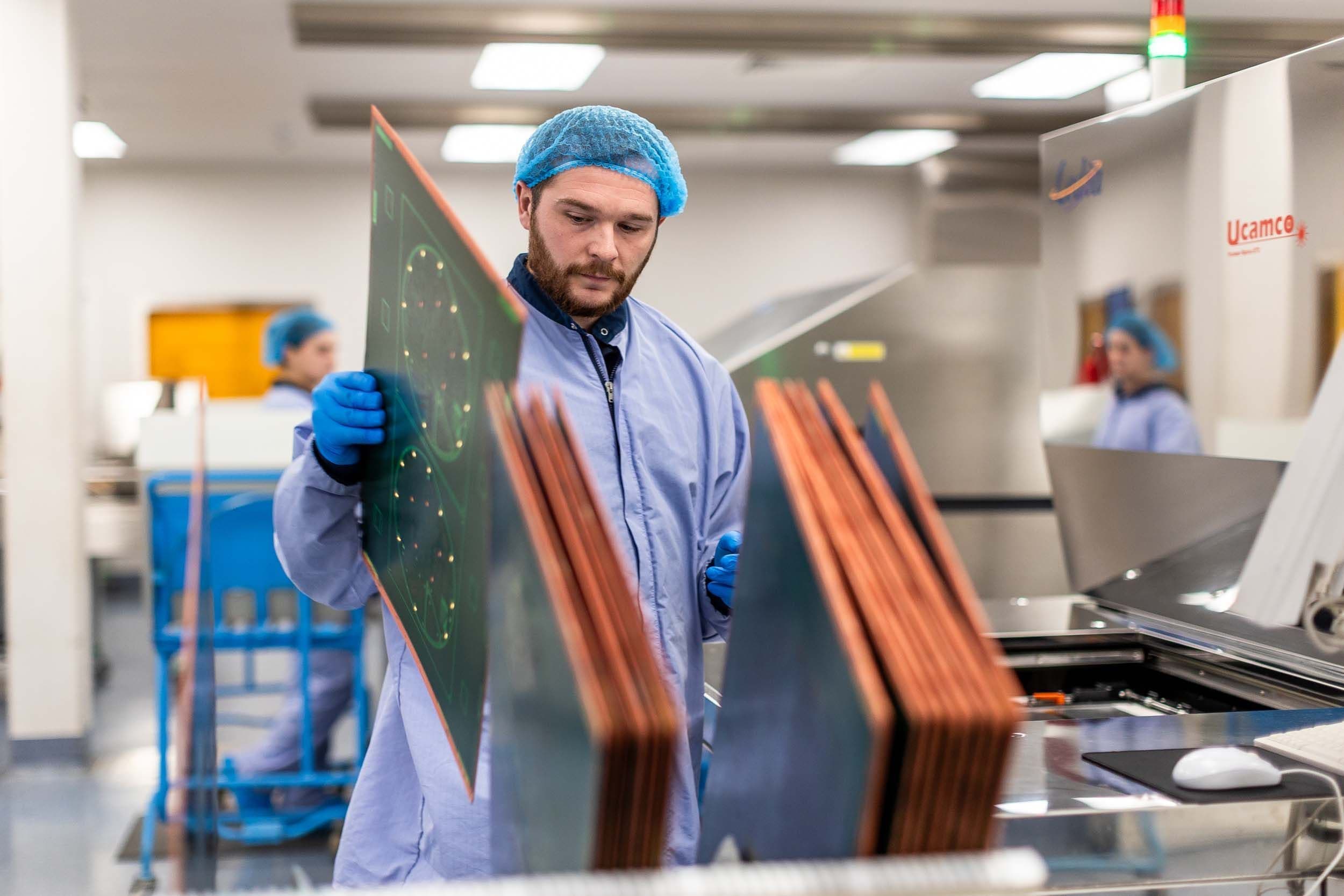
An Exception PCB technician storing green circuit board panels into a protective green slot rack cart.

Why UK Manufacturing Matters for Sovereign Capability

UK-based PCB manufacturing is no longer just a sourcing choice, it is a strategic way to reduce supply chain risk, protect sensitive programmes, improve lead times and strengthen sovereign capability in high-technology electronics.

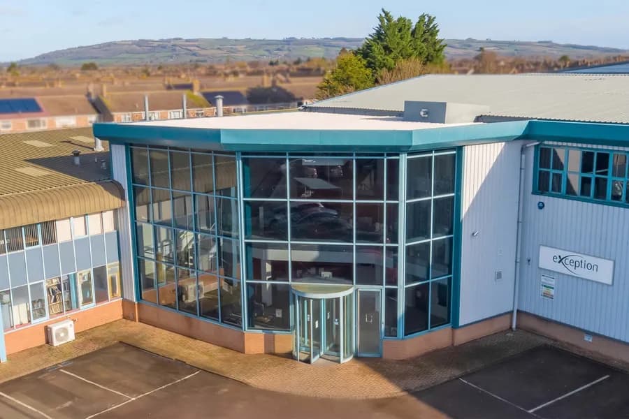
Exception PCB manufacturing facility in Tewkesbury, UK, supporting high-technology printed circuit board production.

Exception PCB Brought Back into British Ownership

Wright Industries has acquired Exception PCB, returning the Tewkesbury-based PCB manufacturer to UK ownership as part of the Connexion Technologies group, strengthening national manufacturing resilience.

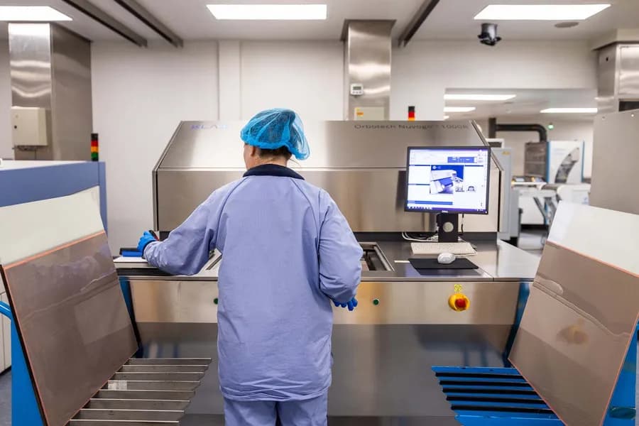
Exception PCB operator at the Orbotech Nuvogo 1000R laser direct imaging system in the cleanroom imaging area at the Tewkesbury facility

Exception PCB Installs Orbotech Nuvogo 1000R Direct Imager

Exception PCB has installed the Orbotech Nuvogo 1000R, a laser direct imaging system that strengthens our capability for fine line, HDI, flex and rigid-flex PCB production at our Tewkesbury facility.

RELATED PCB SERVICES

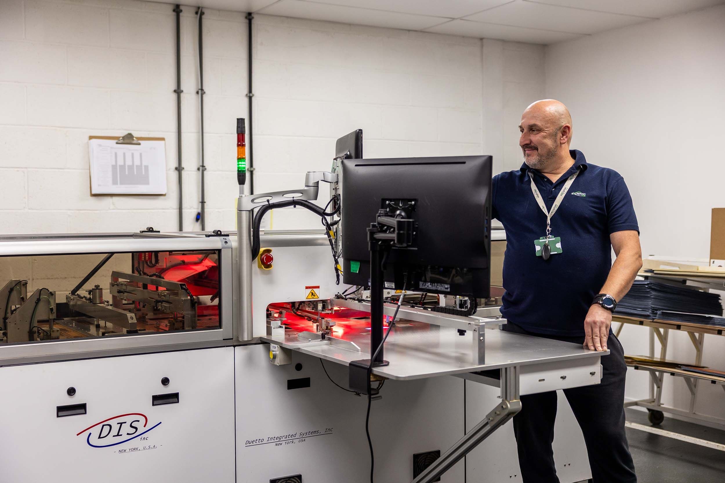
A smiling senior technician standing next to a Duetto Integrated Systems multilayer bonding machine at Exception PCB.

Research & Development

Exception PCB provides comprehensive engineering-led R&D support for new PCB materials and novel stack-ups. Our dedicated R&D team guides customers from initial requirements through to production-ready qualification and UL certification.

PCB manufacturing operator handling large printed circuit board panels during inspection at Exception PCB’s UK facility.

UK PCB Manufacturing

Exception PCB manufactures complex printed circuit boards from our 58,000 sq. ft. facility in Tewkesbury. Engineering-led process control, full traceability, and UK supply-chain resilience for regulated and performance-critical sectors

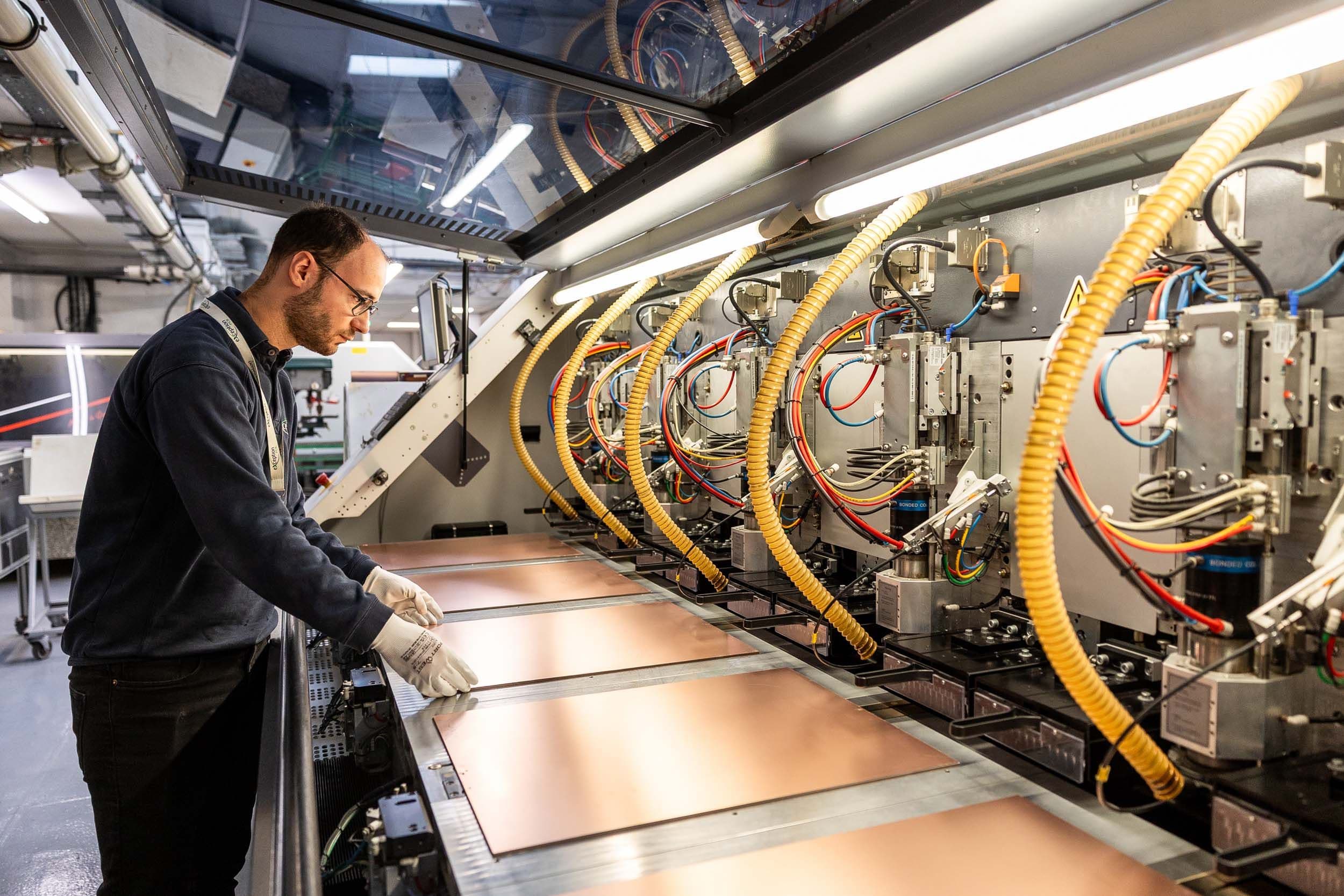
An Exception PCB technician loading copper production panels into a multi-station Schmoll CNC drilling machine.

Quick-Turn PCBs

Exception PCB's quick-turn service delivers accelerated PCB manufacturing for time-critical prototype and production builds, with the same process control and quality discipline applied to every order.

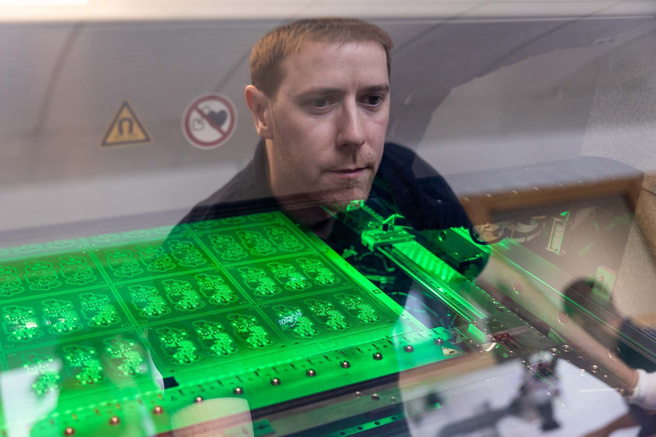
An Exception PCB technician looking through a protective glass window at an illuminated circuit board panel.

PCB Prototyping

Engineering-led PCB prototyping from our UK facility, supporting design validation, NPI, and low-volume manufacture for complex and high-technology applications. Every prototype is built to production-intent standards, reducing programme risk.