
PCB Technical Capabilities
A practical guide to our PCB manufacturing capabilities, tolerances, materials, and processes. Use it to qualify Exception PCB as a supplier, review design requirements, and prepare projects for manufacture.
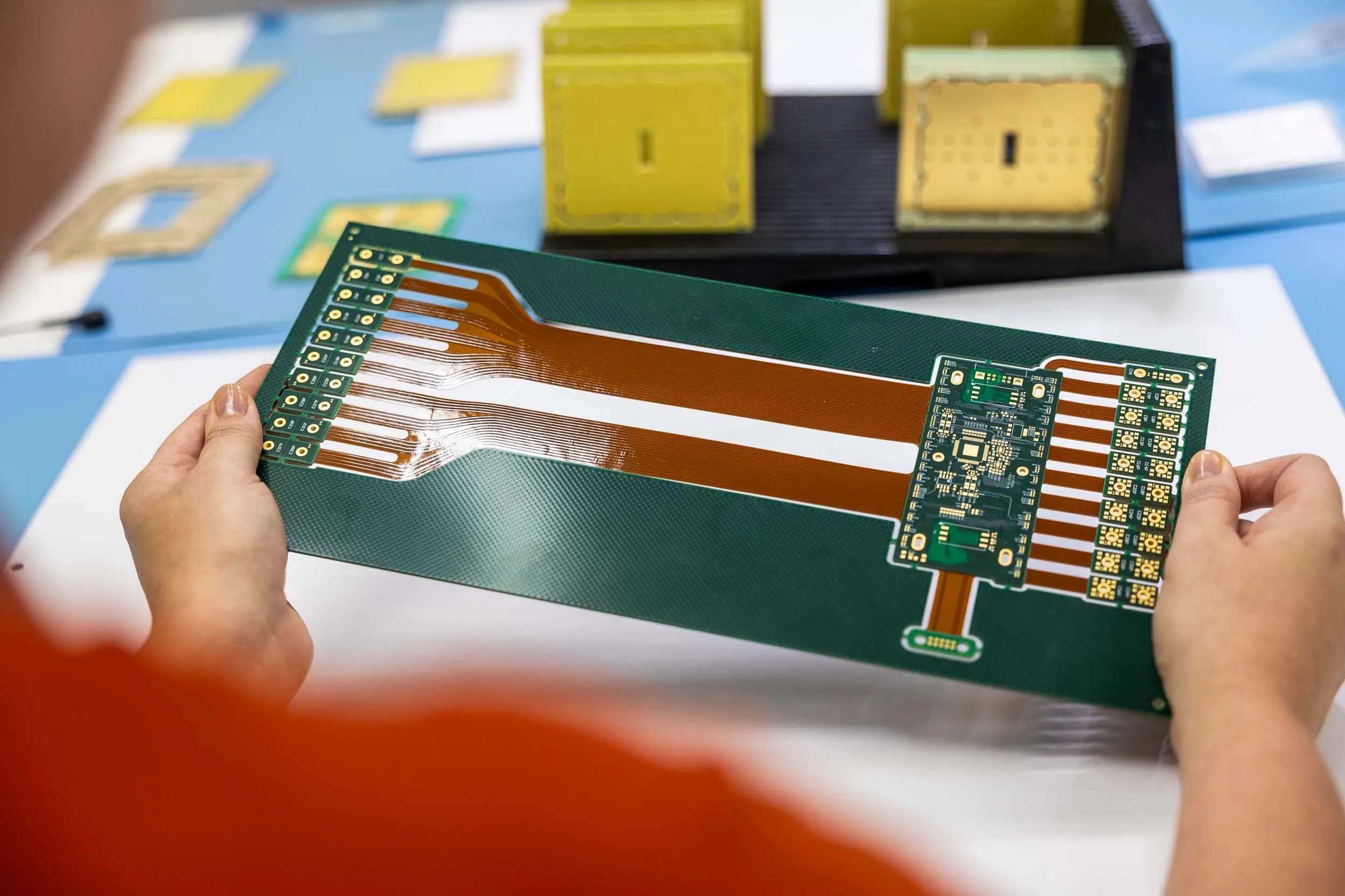
Engineering-led flex and rigid-flex PCB manufacturing from our UK facility, supporting space-constrained, mechanically demanding, and high-technology electronic systems.
Flex and rigid-flex PCBs allow electronic designs to move beyond the constraints of rigid construction, enabling three-dimensional layouts, reduced connector counts, and improved reliability in space-limited or dynamically loaded assemblies. At Exception PCB, flex and rigid-flex manufacturing is built around careful material selection, controlled lamination, and precise CNC machining to maintain structural stability across both rigid and flexible regions.
Our engineers review each design before fabrication, assessing stack-up construction, bend radius requirements, and transition zone geometry to ensure the build is both manufacturable and durable.
Find answers on material systems, bend radius requirements, layer counts, and transition zone tolerances.
The following specifications provide an overview of the manufacturing capability available for flex and rigid-flex PCB builds at Exception PCB. These parameters reflect the process windows supported by our production infrastructure and engineering controls.
| CAPABILITY | ADVANCED CAPABILITY |
|---|---|
| Maximum panel size | 406 × 559 mm |
| Rigid-flex layer count | Up to 24 layers |
| Flex layer count | Up to 12 layers |
| Rigid-flex board thickness | 0.6 mm – 6 mm |
| Flex board thickness | 0.14 mm – 0.7 mm |
| Track / gap capability | Down to 60 µm (advanced process) |
| Microvia laser drill size | Down to 75 µm |
| Mechanical drill size | Down to 0.105 mm |
| Through-hole aspect ratio | Up to 14:1 |
| Microvia aspect ratio | Up to 1:1 |
| Copper via filling | Supported |
| Resin via filling | Supported |
| Electrical testing | 100% electrical test |
| Drilled hole to flex-rigid interface | Minimum 0.8 mm |
These capability ranges allow Exception PCB to support complex rigid-flex designs incorporating multilayer flex circuits, HDI structures, and controlled impedance routing within a single integrated build.
Engineering review ensures the selected stack-up, materials, and routing geometry remain within stable manufacturing limits while supporting the electrical and mechanical performance required by the application.
READY TO DISCUSS YOUR FLEX OR RIGID-FLEX DESIGN?
Our engineers can review your stack-up construction, bend radius requirements, and material selection to confirm your design is both manufacturable and durable.
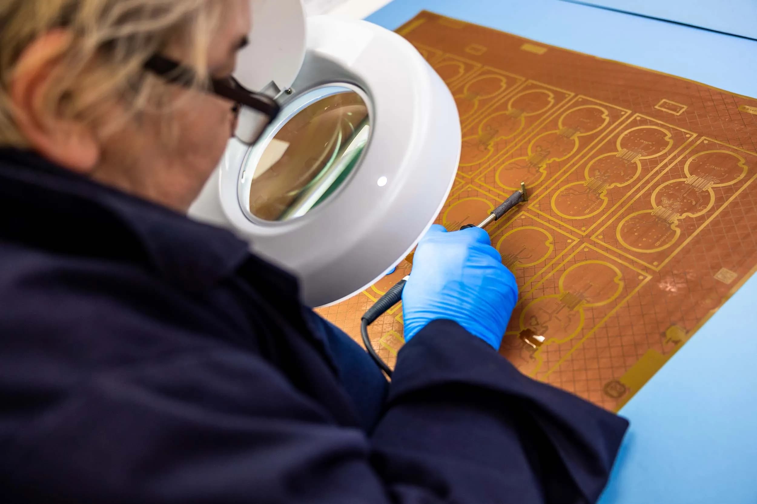
Material selection is fundamental to flex and rigid-flex reliability. Laminates and prepregs must support automated assembly, meet flexibility requirements in the bend areas, and be compatible with each other and with the manufacturing processes involved.
Exception PCB works with a wide range of material systems including:
Stack-up design for flex and rigid-flex requires careful consideration of copper distribution, layer symmetry, and the transition between rigid and flexible regions. Getting this right during the design stage reduces manufacturing risk and improves long-term reliability.
Flexible circuits demand the same level of inspection discipline as rigid multilayer boards, while also accounting for the mechanical behaviour of flex materials.
OUR QUALITY CONTROL PROCESSES INCLUDE:
Inspection data is used to confirm that the finished structure matches the intended stack-up and that copper geometry remains within tolerance.
Our engineers can review your stack-up, material selection, and bend radius requirements before the design is finalised.
Flex and rigid-flex circuits are designed for environments where traditional rigid PCBs and discrete interconnects cannot meet the space, weight, or reliability demands of the application.

AEROSPACE AND SPACE ELECTRONICS
Airborne and spacecraft assemblies require flex circuits that maintain electrical performance through sustained vibration, wide temperature cycling, and a service life that cannot be interrupted for replacement or repair. Material selection and copper construction are critical to long-term flex endurance.

MEDICAL INSTRUMENTATION
Implantable and handheld medical devices use rigid-flex construction to reduce connector count, minimise assembly failure points, and meet the strict dimensional constraints of miniaturised enclosures. Manufacturing traceability and process consistency are non-negotiable for medical-grade builds.

RF AND COMMUNICATIONS SYSTEMS
Flex circuits used within RF assemblies require controlled impedance routing and consistent dielectric properties across the flexible section. Maintaining electrical performance through bend cycles demands precise laminate selection and manufacturing discipline.

MOTORSPORT ELECTRONICS
Control electronics in motorsport and automotive applications face high vibration, thermal shock, and compact packaging requirements. Rigid-flex construction reduces mechanical interconnection points and improves system reliability in demanding operating environments.
Flex and rigid-flex projects benefit significantly from early manufacturing input. Many reliability risks originate during the design stage rather than during fabrication.
Addressing these factors early reduces risk during manufacturing and avoids costly redesign cycles later in the programme.
EXCEPTION PCB ENGINEERS WORK WITH DESIGN TEAMS TO REVIEW:
TALK TO OUR ENGINEERS
Our engineering team can review your flex or rigid-flex stack-up, material selection, and manufacturability before production begins.
Below we have answered the questions our engineers are asked most often. If yours isn't covered, get in touch with the team directly.
Rigid-flex reliability is primarily influenced by material selection, copper thickness within flex regions, bend radius design, and control of the rigid-to-flex transition.
Mechanical stress tends to concentrate at transition zones or bend areas. Stack-up symmetry, balanced copper distribution, and appropriate coverlay protection help ensure the circuit can tolerate mechanical movement and thermal cycling over the lifetime of the product.
Engineering review during stack-up definition is one of the most effective ways to mitigate these risks.
Copper fatigue within bend regions is the most common long-term failure mechanism in pure flex designs.
This typically occurs when the bend radius is too small relative to copper thickness, or when copper traces are routed in ways that concentrate mechanical stress during movement.
For rigid-flex circuits, the most common cause of failure shifts from copper fatigue to delamination and copper trace damage at the rigid-to-flex interface. This area is the highest stress point in the entire assembly.
Reliable flex designs ensure that:
These factors significantly increase the operational life of the circuit.
Yes, HDI features such as laser-drilled microvias and sequential lamination structures can be incorporated into rigid-flex builds.
However, careful engineering review is required to ensure that HDI features remain compatible with flexible materials and lamination processes.
The stack-up must support both:
This balance is critical when integrating HDI with polyimide flex circuits.
Manufacturing input is most valuable during early stack-up and layout planning.
Flex and rigid-flex designs often require adjustments to:
Addressing these factors early helps avoid redesign cycles later in the programme.
Most flexible circuits use polyimide-based materials due to their thermal stability and mechanical durability.
Rigid-flex structures typically combine polyimide flex layers with rigid laminate materials, allowing complex multilayer architectures that support both mechanical flexibility and high component density.
The advanced capabilities of Exception PCB allow for the integration of flexible materials with a wide selection of specialist resin systems, including ceramic-filled, high-speed, RF, and halogen-free variants.
Material selection must consider mechanical behaviour, lamination compatibility, and long-term environmental performance.
Explore guides and references covering PCB construction types, material selection, and the full range of capabilities available at Exception PCB.
Explore related technologies that support compact, reliable flex and rigid-flex designs, from material selection and HDI structures to controlled via filling.
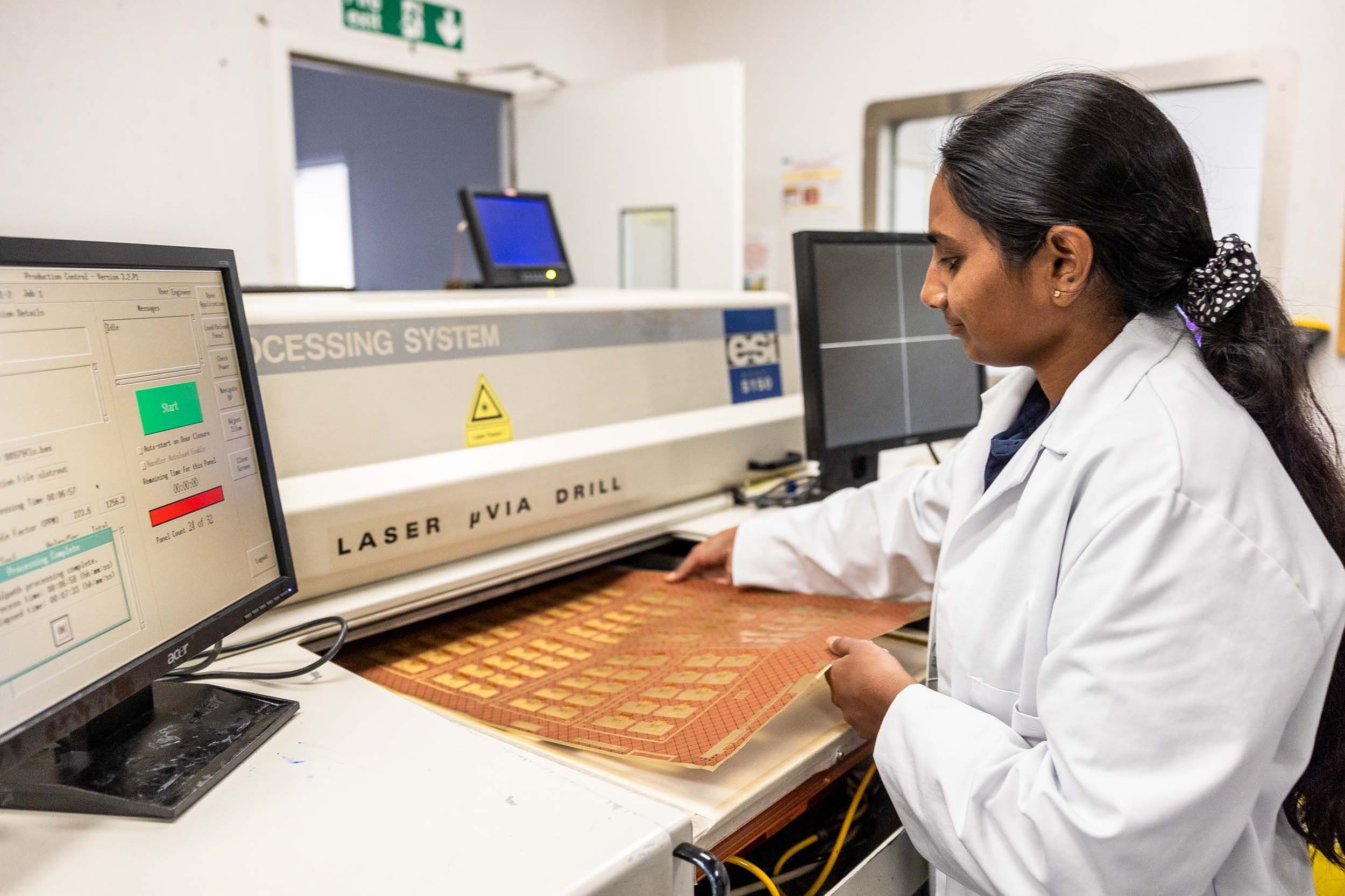
Support for specialist and hybrid PCB materials selected to meet thermal, electrical, and environmental performance requirements in applications where standard FR4 or conventional laminate systems cannot deliver the required performance.
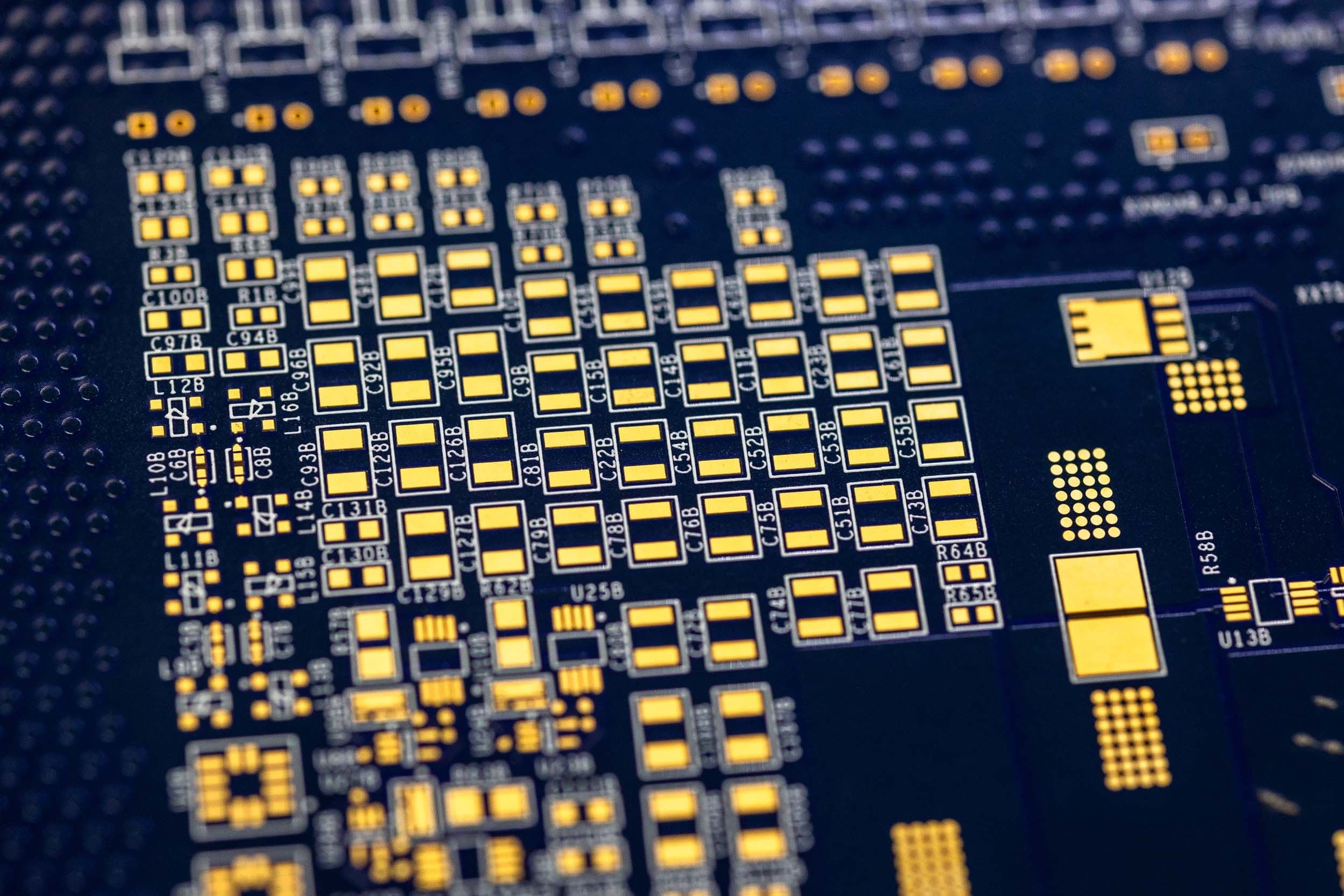
High-density interconnect PCBs for fine features, microvias, and complex multilayer designs, manufactured using production-ready processes with full engineering oversight to ensure reliable and repeatable fabrication of the most demanding constructions.
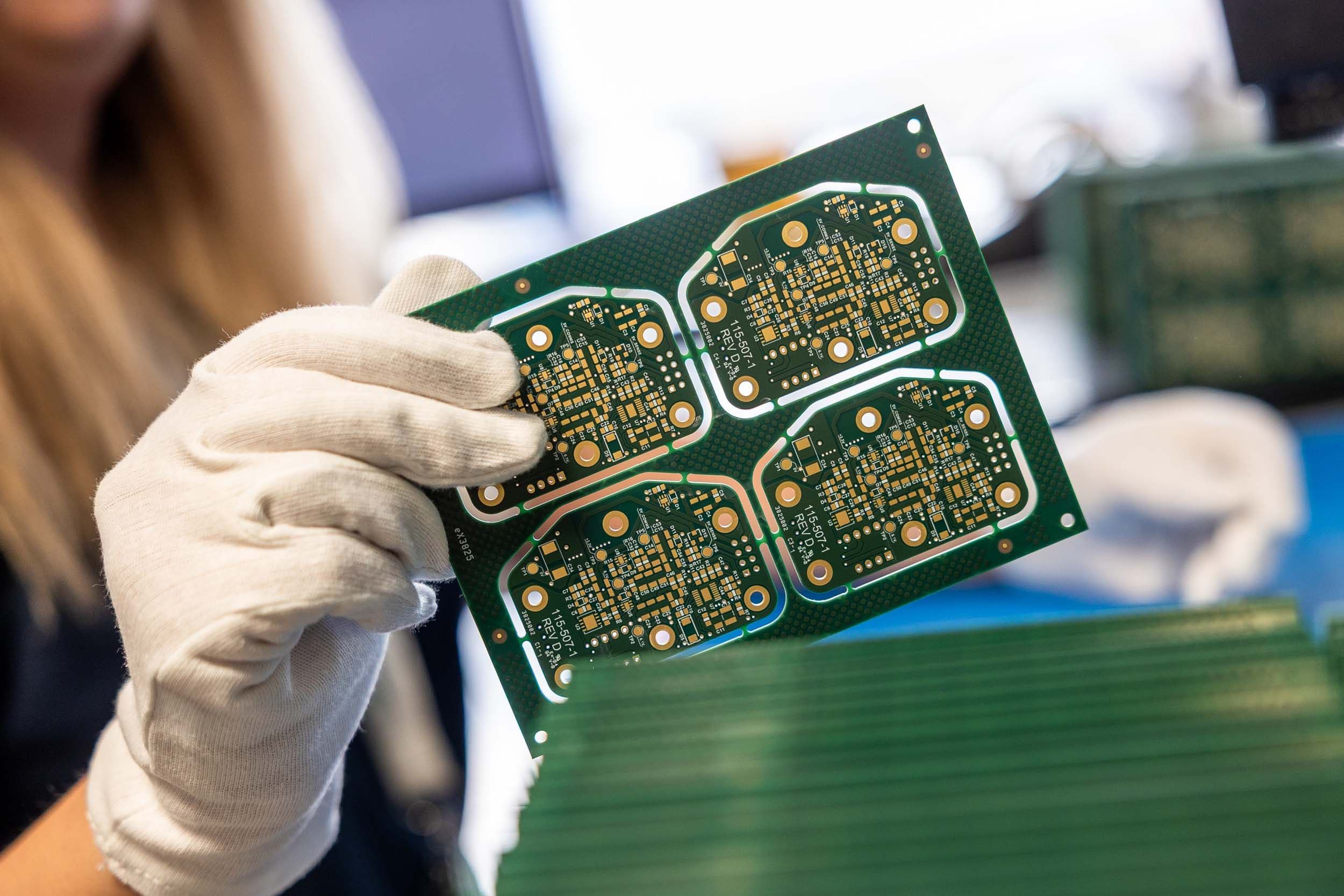
Resin via fill for blind, buried, and through-hole vias, providing consistent surface planarity to support via-in-pad designs, fine-pitch assembly, and sequential lamination builds where assembly quality and via integrity matter.
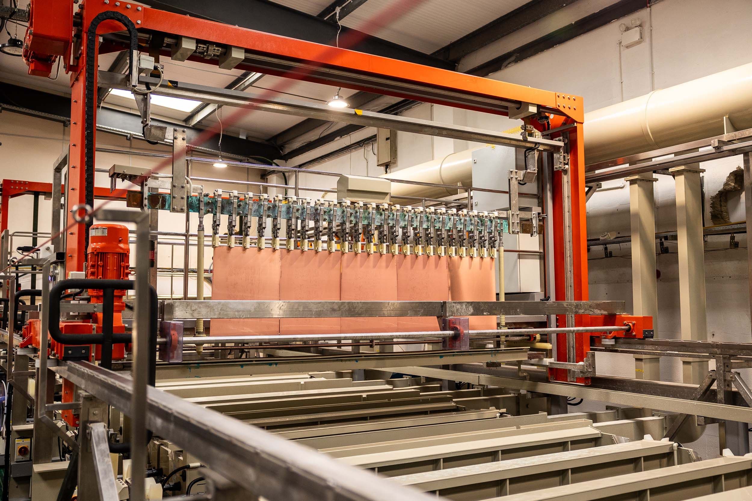
Copper via filling for blind, buried, and through-hole vias, supporting HDI constructions, via-in-pad designs, and thermally demanding multilayer PCBs where electrical continuity, thermal performance, and consistent fill quality are required.
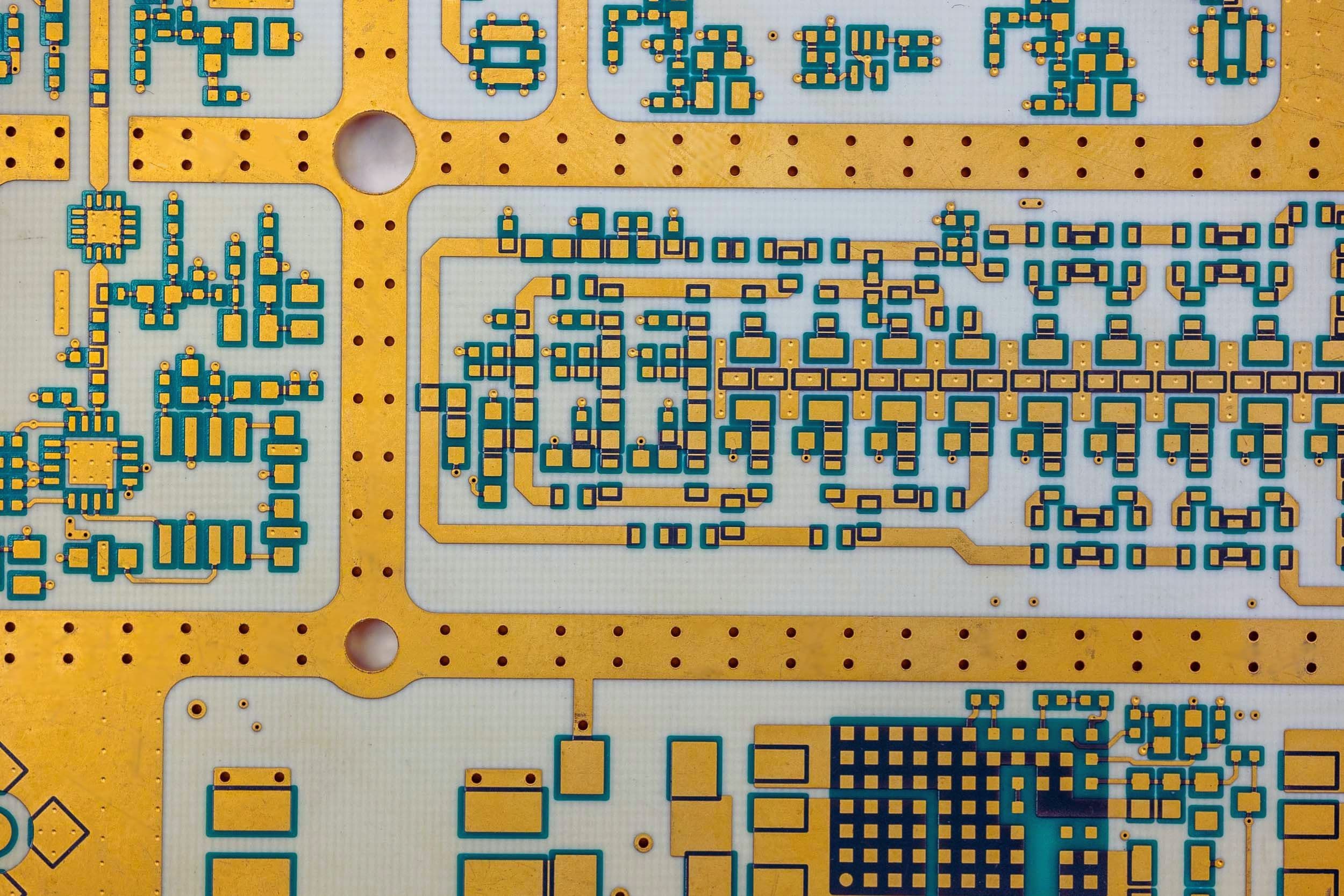
RF and high-frequency PCBs built to support controlled impedance, low-loss materials, and consistent signal integrity in demanding applications where dielectric performance, layer registration, and material choice directly affect circuit behaviour.